Enter the course
This course introduces the reader to RF transceivers for 5G base stations problematics and the approach proposed by consortium of 5G_GaN2 project for 5G networks solution. Individual chapters advise the answers for questions that students may have to gain balanced knowledge.
Development of this e-learn course was funded by HORIZON2020 project 5G_GaN2 (ECSEL-2017-2-RIA № 783274).
| Site: |
eLearn Central |
| Course: |
Advanced RF Transceivers for 5G base stations based on GaN Technology |
| Book: |
Enter the course |
| Printed by: |
Guest user |
| Date: |
Saturday, 20 September 2025, 11:24 AM |
 |
1
Project 5G_GaN2 objectives
|
 |
5G_GaN2 has as major objective to develop new industrial disruptive technologies from semiconductor to integration. It will support the birth of new sub system architecture and allows to target the steps in performances for the 5G generation from Ku to E bands for BTS, point to point & SATCOM communication networks as ilustrated at Fig. 1.1.
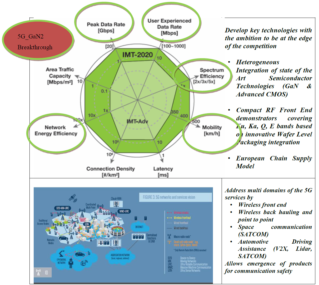
Fig. 1.1: Key challengs for 5G and contributions from 5G_GaN2 project
 |
2
Motivation
|
 |
The communication network will undergo tremendous changes in the future years, in relation with 2 main drivers:
- Strong increase of data linked to new demand trends: high resolution video, virtual and augmented reality etc.
- Emergence of the Internet of Things (IoT), considered as the “3rd wave of internet” with 30 billion devices to be connected by 2020.
The data per month is expected to double from 2016 to 2019, reaching 166 exabytes in 2019 (Source: Cisco VNI Mobile, 2016, see graph hereafter on Figure 2.1).
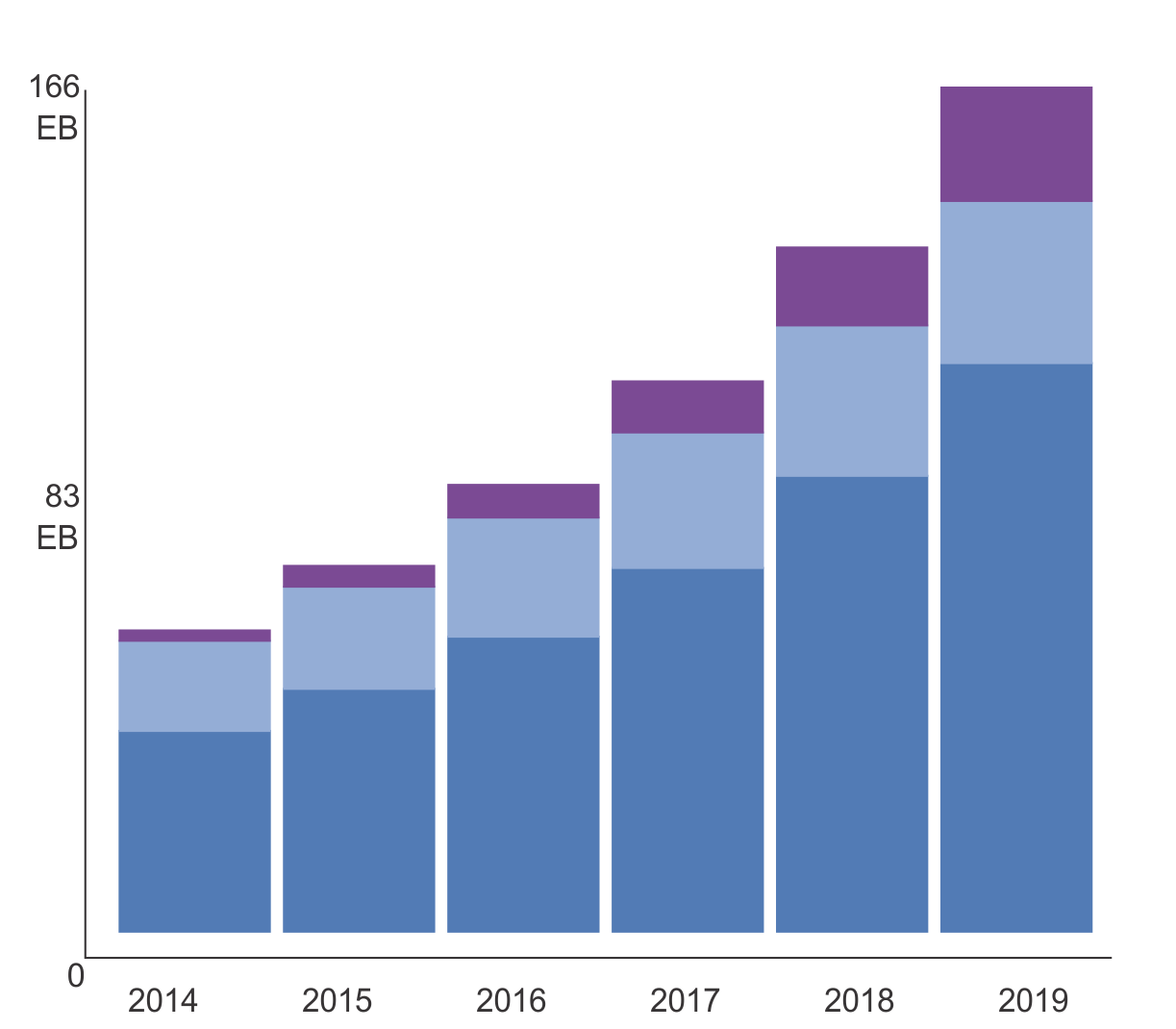
Fig. 2.1: Forecast global IP traffic per Month of Data (Source: Cisco VNI Mobile, 2016)
It appears in this graph that, among the different types of data (fixed internet, managed IP and Mobile data) mobile data will undergo the highest growth, with a CAGR of 53% from 6.2 exabytes in 2016 to 30.6 exabytes in 2019. To cope with such growth and with the deployment of new type of devices and applications, modifications to the network appears essential, in particular to better support features like: low latency, better coverage, multi-standard compatibility, high power efficiency, high reliability and dependability.
As a consequence, the use of RF transceivers is expected to undergo radical changes in the future years with the use of higher frequency and larger bandwidth. A typical coverage scheme is shown in Figure 2.2.
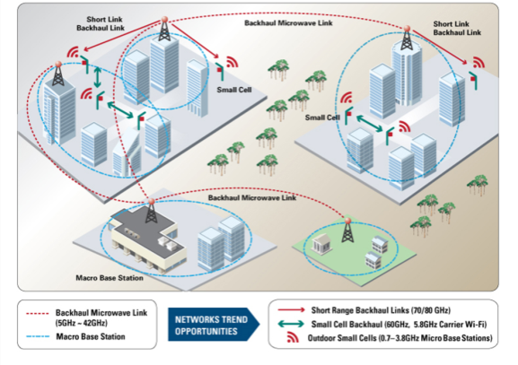
Fig. 2.2: The Evolution & Economics of E-Band for Wireless Backhaul (Source: D.Richardson, Product Line Director, Wireless, MACOM)
The RF network relies on different types of “cells” (i.e. RF transceivers) designated in relation with the radius / range:
- Femtocell: 10 m
- Picocell: 200 m
- Microcell (or metrocell): 2 km
- Macrocell: 10 km
While the femto/picocells needs will be mostly covered by the CMOS or bi-CMOS technology (and its foreseen evolution), micro/macrocells needs are much more challenging in terms of frequency, bandwidth, power, power efficiency and linearity.
 |
3
How to achieve the objectives?
|
 |
The consortium of 5G_GaN2 project believes that silicon (Si) based technology and its foreseen evolution will not be in a position to fulfil these needs. Gallium Nitride (GaN) based technology for microwave applications appears now as the most credible solution; moreover, from an industrial perspective, its credibility is now established thanks to the recent set-up of GaN industrial facilities in Europe (UMS).
In the past years, significant effort has been invested to the research and development GaN HEMT technologies with emphasis on technological building blocks. Key applications demonstrators with wide band gap technologies has confirmed a breakthrough in the field of RF emission/reception functions, keeping in mind reliability aspects. Applications covering frequencies from low MHz to below 20 GHz were targeted and commercialization of suitable components is currently underway.
If professional and defence applications have been strongly supporting GaN technology at its dawn, there are now a booming market for wireless telecommunications requiring to reach higher operation bands together with larger bandwidths.
An additional step is therefore now necessary to access higher frequencies power technologies, pushing the limits of GaN devices into the millimetre wave range with required electrical efficiencyand linearity to address 5G, SATCOM, Cable TV, and more globally the high data rate wireless market and future markets.
 |
4
What are the demands?
|
 |
According to today’s discussions in the standardisation bodies, 5G wireless communication networks will for the first time additionally resort to high bit rate mm wave-communication technologies not only for small cell front-/back-haul, but as well for short range access. The discussions around the carrier frequencies and other communication parameters have not settled yet, though we can expect that such links will target for bit-rates of 10 Gbit/s or beyond and will cover shorter ranges of 1-100 m perhaps. The following chart on figure 3.1 gives the spectral allocations in the 5G emphasis the targeted frequency bandwith.
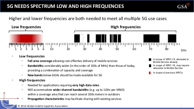
Fig.4.1: Foreseen 5G spectral allocation
Beyond extending operation to higher frequencies, there are several other key technology components relevant for the evolution to 5G wireless access. These components include access/backhaul integration, device-to-device communication, flexible duplex, flexible spectrum usage, multi-antenna transmission, ultra-lean design, and user/control separation.
5G_GaN2 project will play a major role in part of these by developing also key technologies.
 |
4.1
Access/Backhaul integration
|
 |
Wireless technology is already frequently used as part of the backhaul solution. Such wireless-backhaul solutions typically operate under line-of-sight conditions using proprietary radio technology in higher frequency bands, including the millimeter wave (mmW) band.
In the future, the access (base-station-to-device) link will also extend to higher frequencies. Furthermore, to support dense low-power deployments, wireless backhaul will have to extend to cover non-line-of-sight conditions, similar to access links.
In the 5G era, the wireless-access link and wireless backhaul should not therefore be seen as two separate entities with separate technical solutions. Rather, backhaul and access should be seen as an integrated wireless-access solution able to use the same basic technology and operate using a common spectrum pool. This will lead to more efficient overall spectrum utilization as well as reduced operation and management effort.
 5G_GaN2 will address exactly this point by covering Back hauling high frequencies (39 & 80 GHz) full integrated RF transceivers compatible of reduced footprint design Antenna.
 |
4.2
Flexible duplex
|
 |
Frequency Division Duplex (FDD) has been the dominating duplex arrangement since the beginning of the mobile communication era. In the 5G era, FDD will remain the main duplex scheme for lower frequency bands. However, for higher frequency bands – especially above 10GHz – targeting very dense deployments, Time Division Duplex (TDD) will play a more important role. In very dense deployments with low-power nodes, the TDD-specific interference scenarios (direct base- station-to-base-station and device-to-device interference) will be similar to the ‘normal’ base-station-to-device and device-to-base-station interference that also occurs for FDD. Furthermore, for the dynamic traffic variations expected in very dense deployments, the ability to dynamically assign transmission resources (time slots) to different transmission directions may allow more efficient utilization of the available spectrum.
 5G_GaN2 will address exactly this technology feature by evaluating GaN technologies with reduced memory effect.
 |
4.3
Multi-antenna transmission
|
 |
Multi-antenna transmission already plays an important role in current generations of mobile communication and will be even more central in the 5G era, due to the physical limitations of small antennas. Path loss between a transmitter and receiver does not change as a function of frequency, as long as the effective aperture of the transmitting and receiving antennas does not change. The antenna aperture does reduce in proportion to the square of the frequency, and that reduction can be compensated by the use of higher antenna directivity. The 5G radio will employ hundreds of antenna elements to increase antenna aperture beyond what may be possible with current cellular technology.
In addition, the transmitter and receiver will use beamforming to track one another and improve energy transfer over an instantaneously configured link. Beamforming will also improve the radio environment by limiting interference to small fractions of the entire space around a transmitter and likewise limiting the impact of interference on a receiver to infrequent stochastic events. The use of beamforming will also be an important technology for lower frequencies; for example, to extend coverage and to provide higher data rates in sparse deployment.
 5G_GaN2 will propose a key breakthrough fulfilling this requirement. By proposing a Wafer Level Packaging integration of Heterogeneous technologies, it will support exceptionally dense packaging compatible of 3D Antenna integration.
 |
5
Proposed concept
|
 |
To support the demand in increasing peak and mobile data rate, 5G oriented systems are moving to higher frequencies. This trend requires semiconductor and packaging technologies being able to sustain:
- New architecture (beam wave forming)
- Compact RF transceiver compatible of the antenna mesh or system
- Specific design and integration intimately linked to the antenna panel
- Step up in integration to reduce RF losses at minima and improved performances
- Cost Reduction
- Mid to Mass market needs
- Flexibility and reconfiguration
These elements support the push a new strategy of integration. This is observed in many domains and market segments. It explains the participation in this project of key end users covering a large domain on the communication market.
This analysis supports the development of a technology platform having the capability to integrate different front end or Heteregenous technologies at Wafer Level. This approach has many advantages covering technical and business opportunities in Europe taking care of the industrial network requesting low to intermediate volume. The Concept proposed is “One Chip – One Front End RF” as shown in Fig. 5.1.
Fig. 5.1: Objective: One Chip – One Front RF with Heteregeous integration
No equivalent technology platform is already operating at industrial level in Europe and even in the World. We emphasize that this project plan to identify, develop all the R&D activities necessary to push technologies at the right level of readiness in line with this concept.
 |
6
What shall be done?
|
 |
The proposed concept represents a breakthrough in many domains with at lot of technical miletones to solve. In Fig. 6.1 are ilustrated technology approaches (green) to achieve desired product properties (blue).
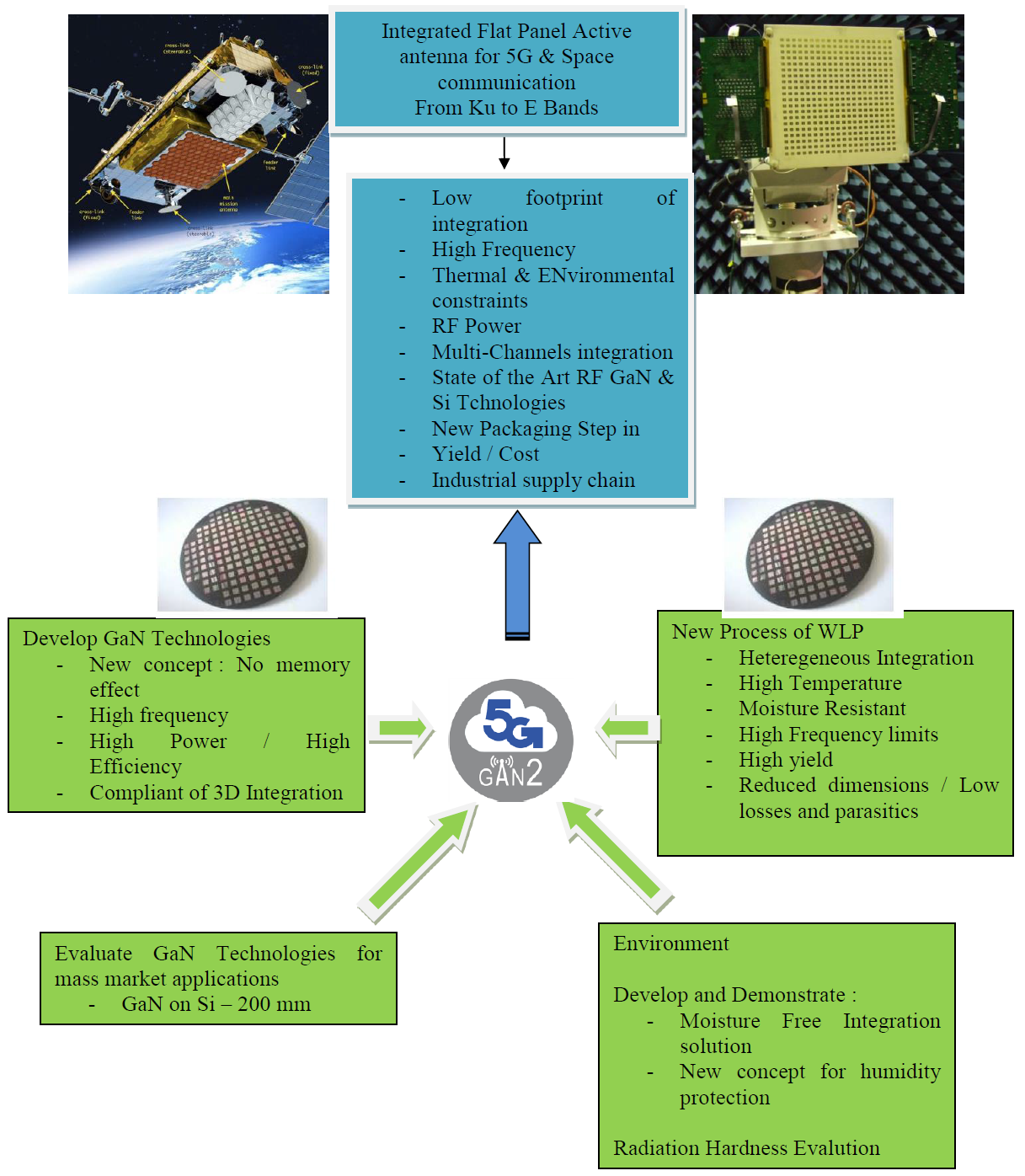
Fig. 6.1: Concept covered by 5G_GaN2: What in blue – Approach in Green
 |
6.1
GaN HEMT technology
|
 |
GaN compound semiconductor devices are now used widely. They have been first used in optoelectronic in blue LED and Blue laser. These materials are now utilised in HEMT for microwave and also in power electronic for DC-DC power conversion.
Indeed GaN technologies have demonstrated exceptional microwave output power performances versus frequency factor of merit with proven reliability for processes mainly below 18 GHz and they are already available on the commercial market. These performances are mostly relying on high breakdown electric field (x10 compared to Si) and electron drift velocity. Fig. 6.2 shows process technology comparison of major semiconductor material used for microwave application as a function of frequency and GaN clearly surpasses all of them.
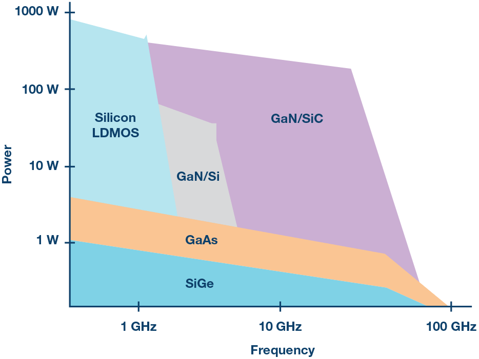
Fig. 6.2: A process technology comparison of microwave frequency range power electronics.(1)
Fig. 6.3 shows the state-of-the-art of GaN MMIC amplifier output powers and output densities versus frequency. Highest reported results are reaching 15W in Ku band (14 GHz), 8W in Ka-Band (30 GHz) and 2W in E-Band (90 GHz). For the GaN technology, the reader has to be aware that the published results are generally reported in scientific journals and conferences and one has to be cautious regarding the actual performance in to-be-announced commercial products. Main companies addressing this segment are US (Wolfspeed (ex-Cree), Qorvo (merge of RFMD and Triquint), MACOM), Japanese (Sumitomo Elec., Fujitsu, Mitsubishi) or European (UMS, OMMIC). Except 2 (MACOM & OMMIC claiming to use also Si substrate), all companies have been developing GaN on SiC substrates for thermal dissipation considerations – SiC has a thermal conductivity of 450 Wm-1 K-1, i.e. similar to copper at room temperature, i.e. 3 time better than Si. Best GaN results are all today obtained using SiC substrates.
It is important to recall to the reader that microwave power and power electronic are quite different in terms of power dissipation. Microwave devices are dissipating a lot due to CW operation with efficiencies degrading as the frequency rise. In case of power electronic dissipation exists only during the switching period and efficiency may reach 99% in pulse compared to below 50% at CW 30GHz.
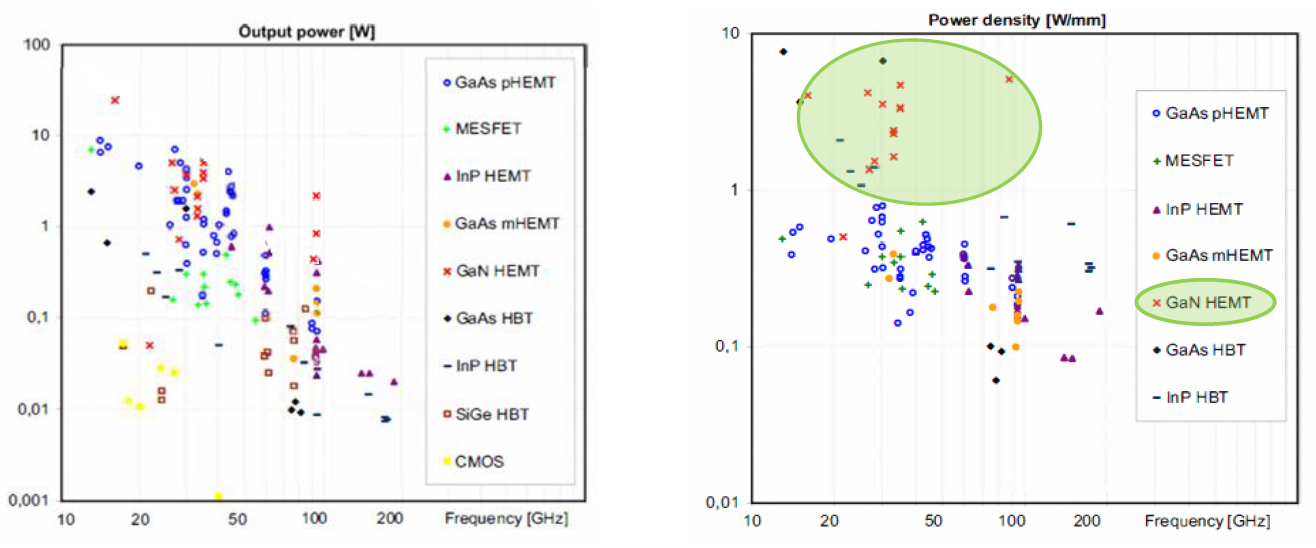
Fig. 6.3: State-of-the-art of GaN MMIC amplifier (for GaN: scientific publication – not commercial specifications), a) Saturated output power in frequency for PA MMIC, b) Power density in frequency for PA MMIC
0.5μm and 0.25μm GaN/SiC HEMT technologies are mature at UMS and now qualified. These device families can be used for frequencies up to 18GHz. This upper frequency is therefore too short for coming telecom markets (c.f. Figure 4). Developments are currently underway at UMS with the support of III-V Lab and IAF to give rise to devices compatible with circuits working up to 35GHz, or even 45GHz using 0.1μm-0.15μm gate lengths. UMS is capitalizing on his former GaN/SiC technologies and their new coming 0.15μm will benefit from their expertise. There is however a large effort to be put before reaching product level. Indeed such development will face challenge like short channel effect, parasitic capacitance, transconductance maximisation, dispersive effect (lag), device topology optimisation, etc. This approach will be the main path to reach state of the art 5G circuits up to 35 GHz. It will benefit from available models to be upgraded to shorter gate length and higher frequency. PDK will have to be derived for active devices and passive elements. The second path will be managed by IAF and III-V Lab who has as objective to push GaN technologies to address the demonstrators planned for higher frequencies above 35 GHz. Swegan will be a major supplier of GaN/SiC epiwafers to UMS. Their demonstration of reduced dispersive effects could be an important advantage to deal with expected high linearity 5G requirements.
_______________________________________________________
(1) Keith Benson: GaN Breaks Barriers—RF Power Amplifiers Go Wide and High, in Analog Dialogue 51-09, September 2017, 
 |
6.2
System in package
|
 |
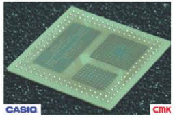
The assembly of the RF transceiver, especially for the TX part (which includes the Power Amplifier) depends on the frequency range and application. Of course, the frequency as well as the power density level are very important criteria, which will define the technology choice for each chip and the overall Packaging architecture. One recent trend observed for many markets is a demand for small size heterogeneous integration (SiP) at low cost. This can be obtained by using organic materials for both the PCB substrate and for the package substrate, as shown in Fig. 6.4.
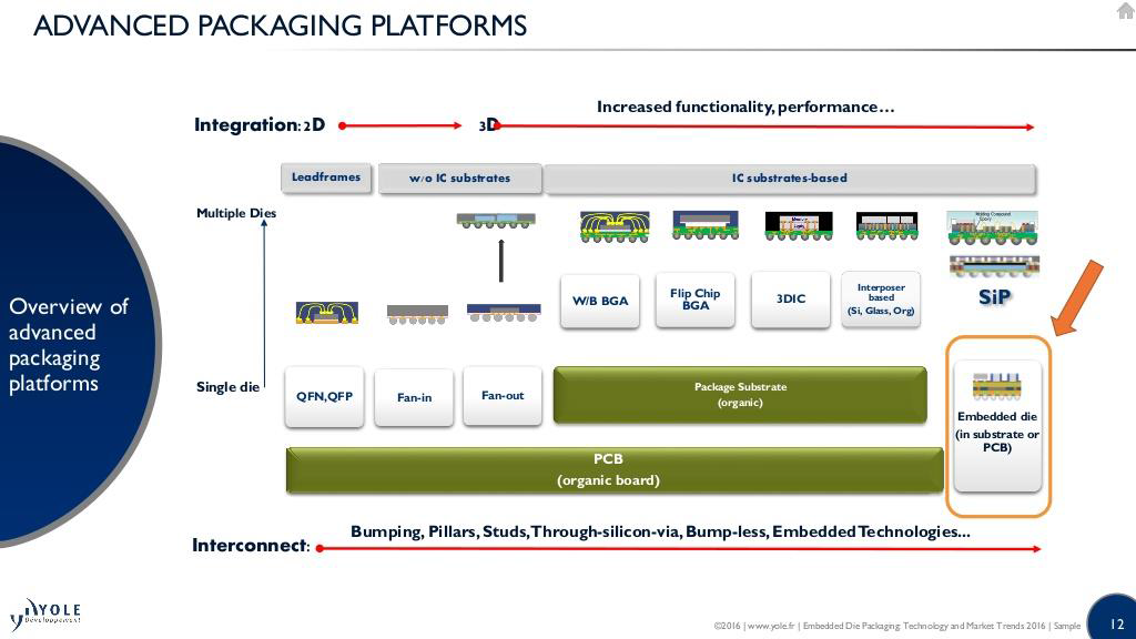
Fig. 6.4: Advanced packaging platforms (source: Yole report, 2016).
System in Package based on organic interposer platform using 3D technologies interconnection is considered as a valid approach for achieving 5G transceiver. It consists in the heterogeneous integration of Silicon CMOS driver chips, GaN Power Amplifier and passive elements in a same package.
The main advantages for this approach are listed below:
- Highly integrated architecture and reduced footprint of the module
- Optimized low loss RF links between the active chips with short interconnects and built-in matching and decoupling network
- Possibility to integrate active and passive elements for decoupling and matching network; at a first stage passive RLC elements and antenna should be considered but active filters and switchers can be also implemented in the interposer in the future
- Wafer level solutions for interconnect and packaging would give competitive advantages in term of aggressive process capability and overall cost in HVM.
In the scope of this project we propose to consider different approaches of packaging for building this SIP module based on organic materials:
- An organic laminate LGA type substrate with chip embedded technology
- A fan-out wafer level packaging using molding compound, also having embedded chip principle.
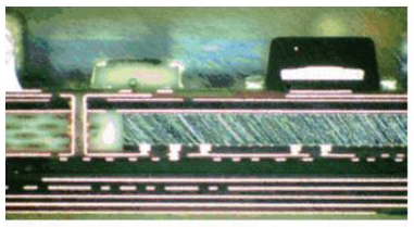
The first approach will be using embedded die technology in organic laminate substrate commonly named “LGA” for Land grid array referring to the termination of the substrate as link to the application board. This technology is already largely adopted in many field of consumer applications as illustrated in these pictures on Fig. 6.5.
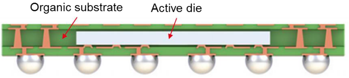
Fig. 6.5: Illustration of embedded die technology in organic laminate substrate.
But, the RF applications considered in this project are still at a development stage. Early development studies can be found in the literature as the work carried out recently at Georgia institute of technology [1] for example. Note that in this work only the GaN Power amplifier is integrated in the organic substrate, our ambition is to integrate a multi-chip module and active and passive elements.
Moreover the aim will be to introduce new added value features to this package to address the specific challenges of mm-wave and high power devices such as RF transmission efficiency and thermal management for example.
The second approach will be using a Fan-out wafer level packaging (FOWLP) technology based on epoxy molding compound material.
Standard eWLB process flow is based on a chip first approach which flow is illustrated hereafter figure 13. It is composed of 2 main blocks:
- Molding strata fabrication with embedded dies
- Fan-out RDL fabrication on top of the strata with can have 1 to plural levels of metal.
On top of last level of metallization UBM is formed for solder ball placement. Cu/solder bumps can be alternatively substituted to solder balls if needed.
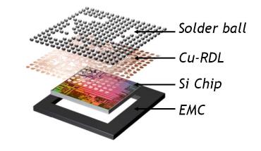
Fig. 6.7: eWLB exploded view (from STAT Chip Pac)
Today another approach has been introduced in the market which is based on RDL first flow described below Fig. 6.8.
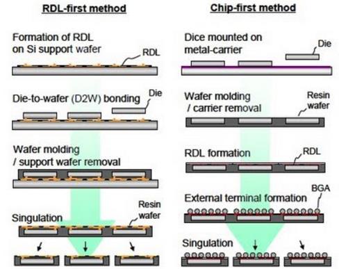
Fig. 6.8: RDL first vs Chipfirst technologies
This last approach allows thinner pitch RDL since the process is done on a rigid carrier substrate on not on the molding material and also offer the advantage of assessing the interposer yield before stacking avoiding to lose good active dies and last it has thinner package capability.
More activities are today pursued on RDL first approach using the fabrication line capability installed in MINATEC including RDL build up, through mold via (TMV) and molding film lamination.
_____________________________________________________________
[1] K. Takinami, "A 60GHz wireless transceiver employing hybrid analog/digital beamforming with interference suppression for multiuser Gigabit/s radio access", 2015 Symposium on VLSI Circuits (VLSI Circuits), June 2015.