GaN/SiC based High Electron Mobility Transistors for integrated microwave and power circuits
This course introduces the reader to GaN/SiC based High Electron Mobility Transistors - basic transistor operation, types of structures, their electrical characteristics, design rules and applications in circuit and system for integrated microwave and power circuits. Individual chapters advise the answers for questions that students may have to gain balanced knowledge.
Development of this e-learn course was funded by HORIZON2020 project OSIRIS (ECSEL-RIA № 662322).
| Site: |
eLearn Central |
| Course: |
GaN/SiC based High Electron Mobility Transistors for integrated microwave and power circuits |
| Book: |
GaN/SiC based High Electron Mobility Transistors for integrated microwave and power circuits |
| Printed by: |
Guest user |
| Date: |
Monday, 15 September 2025, 01:34 PM |

GaN/SiC based High Electron Mobility Transistors for integrated microwave and power circuits
Course for middle school scholars
Authors: Jaroslav Kováč jr., Róbert Szobolovszký, Arpád Kósa, Aleš Chvála, Juraj Marek, Lubica Stuchlíková, Jaroslav Kováč
Institute of Electronics and Photonics, Ilkovičova 3, 812 19, Bratislava, 2015
__________________

This course introduces the reader to GaN/SiC based High Electron Mobility Transistors - basic transistor operation, types of structures, their electrical characteristics, design rules and applications in circuit and system for integrated microwave and power circuits. Individual chapters advise the answers for questions that students may have to gain balanced knowledge.
Development of this e-learn course was funded by HORIZON2020 project OSIRIS (ECSEL-RIA № 662322).
__________________
 1 Motivation
.
Largest family of power devices are GaN based power High Electron Mobility Transistors (HEMTs) having a very important issue, the heat sink out property. The improvement of this parameter, by evolving SiC substrates as suitable candidates for this job, is also the main interest of the project OSIRIS.
Power and microwave Electronics are used to change properties (voltage and current magnitude and/or frequency) of the electrical power to suit a particular application (Fig. 1.1) . It is an interdisciplinary technology.
GaN perhaps shows the greatest promise at high frequencies and high power (Fig. 1.2).
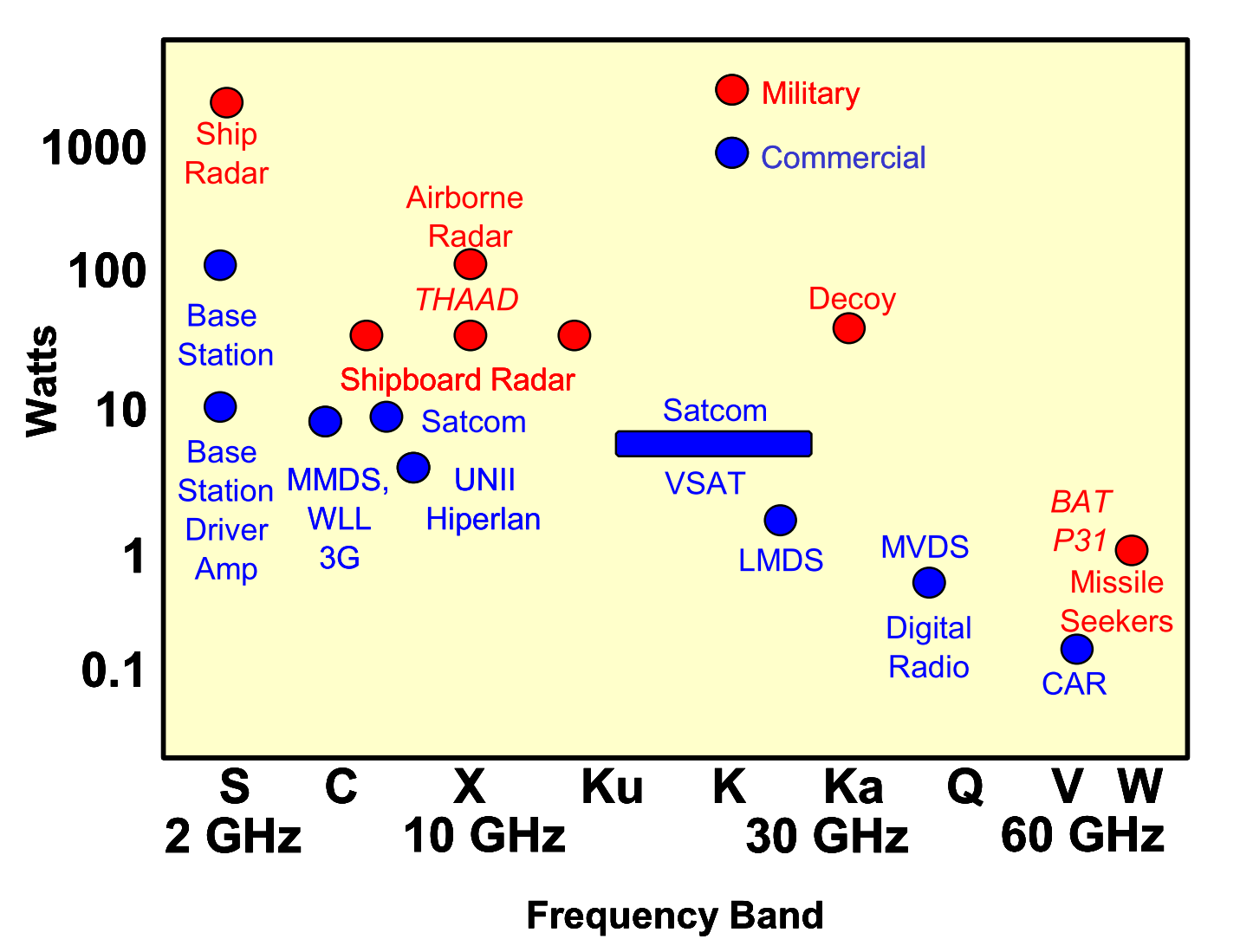
Fig. 1.1 Current Power Device Applications
Mr. B. Jayant Baliga, an Indian electrical engineer best known for his work in power semiconductor devices (Fig. 1.1) wrote: “Power semiconductor devices are recognized as a key component of all power electronic systems. It is estimated that at least 50 percent of the electricity used in the world is controlled by power devices. With the wide spread use of electronics in the consumer, industrial, medical, and transportation sectors, power devices have a major impact on the economy because they determine the cost and efficiency of systems. After the initial replacement of vacuum tubes by solid state devices in the 1950s, semiconductor power devices have taken a dominant role with silicon serving as the base material. These developments have been referred to as the Second Electronic Revolution”.(1)
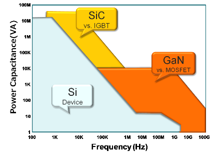
Fig. 1.2 Next generation GaN devices with the advantage in compact, high frequency applications, such as in switching power supply (2)
__________________
| (1) |
BALIGA, B.J. Advanced Power MOSFET Concepts., 2010. 562 s. ISBN 978-1-4419-5916-4. |
| (2) |
Sanken Semiconductors, Next Generation Power Semiconductors: Sanken's Commitment to GaN/SiC Development, [online] 2013, [cit. 2015-10-10] |
 1 Motivation
1.1 Project Osiris
OSIRIS project (Optimal SIC substRates for Integrated Microwave and Power CircuitS)(1), a Research and Innovation Action (RIA), aims at improving substantially the cost effectiveness and performance of gallium nitride (GaN) based millimetre wave components.
OSIRIS project will demonstrate significantly more reliable and higher efficiency devices through an innovative solution by producing GaN High Electron Mobility Transistors (HEMTs) and SiC devices using isotope-enriched, semi-insulating (SI) silicon carbide (SiC) substrates, that manifest higher thermal conductivity and lower costs specifically for GaN microwave applications. The novelty of OSIRIS project is to utilize an ingenious way of increasing the thermal conductivity of the substrate and hence the power efficiency of the HEMT device by removing all but one of the isotopes for Si and C, respectively. The thermal conductivity of the SiC substrate will make a significant leap by about 30% which plays an important role for all devices.
OSIRIS project will allow reinforcing GaN technology penetration into the market by cost effectiveness of the SiC substrates and circuit performances improvement thanks to better heat spreading close to the dissipative area. For microwave GaN/SiC HEMT this isotopic approach could create a complete shift in the currently used substrate / GaN epi-wafer technology; it intends to grow high thermal conductivity (+30%) semi-insulating SiC on top of low cost semiconducting SiC substrates (widely used by the power electronics and LED industries). Reduced layer thickness is necessary as only the top 50 to 100 µm SiC wafer is really useful as the substrate itself is currently thinned to realise microstrip waveguided microwave circuits (Fig.1.3).
For power electronics, this isotopic innovation will be essentially focused on thermal improvement, i.e. better electron mobility at a given power dissipation as mobility and drift mobility decrease with temperature and also better carrier transport thanks to lower scattering rates. Schottky and p-i-n diodes will be tested using this material, which however will have to be doped while microwave devices need semi-insulating materials.
One of the important goals of OSIRIS project is to disseminate discoveries and achievements of current high level research through various ways. Within the mission it is very important to teach young scholars at Middle schools and Universities about state of the art novelties and advanced research inventions.
Fig. 1.3 Comparison of GaN/SiC/Si/GaAs high-power RF transistors, OKI Semiconductors, May 2014(2)
__________________
| (1) |
OSIRIS - Optimal SIC substR ates for Integrated Microwave and Power CircuitS, CORDIS. [online], 2014 [cit. 2015-10-10] |
| (2) |
GaN to grow at 9% CAGR to over 18% of RF device market by 2020, [online] |
 1 Motivation
1.2 Why HEMT?
HEMT is also known as heterojunction Field Effect Transistor (HFET), modulation-doped Field Effect Transistor (MODFET) or Two Dimensional Electron Gas Field Effect Transistor (TEGFET).
Transistors are used in many electronic devices such as switches, amplifiers or oscillators. HEMT transistors are able to operate at higher frequencies (up to millimeter wave frequencies) than ordinary transistors. They are used in high-frequency products such as cell phones, satellite television receivers, voltage converters and radar equipment. Therefore the HEMTs are an important components for high speed and high frequency digital and microwave circuits especially for low noise applications. HEMTs tend to satisfy growing demands of high power, high speed and high efficiency communications (Fig. 1.4).
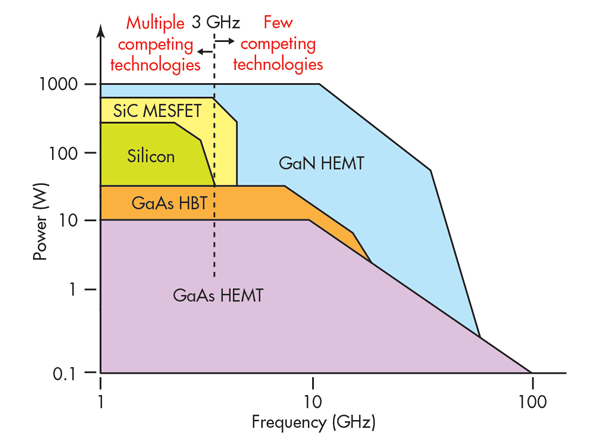
Fig. 1.4 Five different semiconductor technologies vie for RF power-amplifier sockets in various applications, depending on power and spectral requirements.(1)
RF power amplifier is the final active stage that drives the transmitting antenna. Power amplifier designs currently deployed use any of five semiconductor technologies: silicon LDMOS transistors, silicon-carbide (SiC) MESFETs, gallium-arsenide (GaAs) HEMTs, GaAs HBTs, and gallium-nitride (GaN) HEMTs.(1)
__________________
| (1) |
Stephen Oliver, Optimize a Power Scheme for these Transient Times, Sep 30, 2014 [online] |
 1 Motivation
1.3 Course aim
.
The main aim of the course “GaN/SiC based High Electron Mobility Transistors for integrated microwave and power circuits” is to introduce the reader to GaN/SiC based High Electron Mobility Transistors - basic transistor operation, types of structures, their electrical characteristics, design rules and applications in circuits and systems for integrated microwave and power circuits. Individual chapters advise the answers for questions that students may have to gain balanced knowledge and provide basic information about present research in the field of microwave and power electronics and the role of HEMTs in this field.

Fig. 1.6 GaN HEMT applications(1)
__________________
| (1) |
Microsemi Corporation - GaN on SiC HEMT transistor 1011GN-1000V [online] |
 2 HEMT invention
.
2015 marked the 35th anniversary of the High Electron Mobility Transistor invention. The HEMT represented a triumph for the, at the time, relatively new concept of bandgap engineering and nascent molecular beam epitaxy technology. The HEMT showcased the outstanding electron transport characteristics of two dimensional electron gas (2DEG) systems in III-V compound semiconductors.
 Takashi Mimura presented the idea of high electron mobility transistor in 1979 as first on the world. He is working as Fellow at Fujitsu laboratories Ltd., of the Institute of Electronics, Information and Communication engineers (IEICE), Japan. Mimura and his colleges had problems with the growth and manufacturing of the device but in January 1980 they could obtain the characteristics of the world’s first HEMT transistor (Fig. 2.1). The team published their device in March of the same year, as a transistor, that could compete with the conventional GaAs MESFET in high frequency applications(1).
.

Fig. 2.1 Satoshi Hiyamizu (left), and Takashi Mimura (right) testing the first HEMT
__________________
| (1) |
Takashi Mimura, “The Early History of the High Electron Mobility Transistor (HEMT)”, IEEE Transactions on microwave theory and techniques, Vol. 50, No. 3, March 2002. |
 2 HEMTs invention
2.1 History
.
- In the 1979 Takashi Mimura and colleagues developed the first HEMT (AlGaAs/GaAs system) at Fujitsu in Japan. The HEMT was based on the concept of modulation doping first demonstrated by Ray Dingle and his collaborators at Bell Labs in 1978.(1,2)
- In Europe, Daniel Delagebeaudeuf and Trong Linh Nuyen from Thomson-CSF (France) filed for a patent of this device on the 28th of March 1979.(3)
- In 1980 Takashi Minura, Fujitsu laboratories designed the features of the first HEMT.
- In 1981 Fujitsu had demonstrated the first HEMT integrated circuit featuring an enhancement/depletion-mode logic ring oscillator that showed a switching delay of 17.1 ps, “the lowest of all the semiconductor logic technologies reported thus far” (Fig. 2.2).
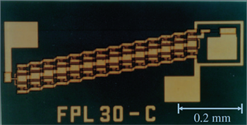
Fig. 2.2 First HEMT integrated circuit: 27-stage ring oscillator
- In 1985 the manufacturing capabilities had grown to such a level that the HEMT structure was announced as the device with the lowest noise characteristics in the world.
Fig. 2.2 First commercial HEMT: cryogenic low-noise amplifier for radiotelescope at Nobeyama Radio Observatory(4)
- In 1987 - Commercialization of HEMTs significantly increased in Japan and Europe and HEMTs began to replace GaAs MESFETs in broadcasting satellite receivers. HEMTs made it possible to reduce the size of a parabolic antenna by one-half or more.
- In 1988 - HEMT multibit data registers(5) were developed for the supercomputer of the National Research and Development Program of Japan.
 Fig. 2.3. HEMT multibit data registers mounted on circuit board of supercomputer.
- Early Applications: Low noise amplifiers (Installed in radio telescope), other space and military applications, satellite broadcasting receivers. The transistor quickly gained popularity and spread all over the world.
- In 1993 Asif Kahn demonstrated the first AlGaN/GaN HEMT.(6)
- Commercial production took off in the 90’s. In the last 30 years, HEMTs have been demonstrated in several material systems, most notably AlGaAs/GaAs and AlGaN/GaN.(7)
__________________
| (1) |
R. Dingle et al., Appl. Phys. Lett. 33, 665 (1978). |
| (2) |
Edward C. Niehenke, The Evolution of Transistors for Power Amplifiers: 1947 to Today, IEEE, 2015, [online] |
| (3) |
US 4471366, Daniel Delagebeaudeuf and Trong L. Nuyen, "Field effect transistor with high cut-off frequency and process for forming same" google patents link |
| (4) |
Takashi Mimura, Development of High Electron Mobility Transistor, Jpn. J. Appl. Phys., Vol. 44, No. 12 (2005), pp. pp. 8263–8268 |
| (5) |
M. Asif Khan et al., Appl. Phys. Lett. 60, 3027 (1992) |
| (6) |
M. A. Khan, A. Bhattarai, J. N. Kuznia and D. T. Olson: Appl. Phys. Lett. 63 (1993) 1214 |
| (7) |
H Xing, S Keller, Y-FWu, L McCarthy, I P Smorchkova, Gallium nitride based transistors, J. Phys.: Condens. Matter 13 (2001) |
 3 HEMT basic
.
For basic understanding of the HEMT operation it is needed to know about formation of the 2DEG an it's properties which is a key component of the HEMT functionality. This knowledge together with HEMT operation and types is explained in this chapter in a way that should be understandable for wide public. Some of the physical backgrounds for the HEMT theory cannot be more simplyfied and is thus more challenging to understand especially theory about formation of the 2DEG.
 3 HEMT basic
3.1. Formation of the 2DEG
.
Basic HEMT structure widely used to explain the formation of 2Deg (two dimensionasl electron gas) consist of a GaN/AlGaN heterojunction. Heterojunction is a special type of junction between two different semiconductors, i.e. it is a junction formed by two semiconductors with different band gaps shown on Fig. 3.2.(1)
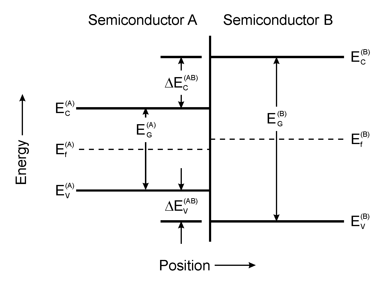
Fig. 3.2 Heterojunction formed between two different semiconductors
By splitting the heterojunction into two separated parts we can easily analyze and understand the formation of the 2DEG. Let’s assume the following that the layer of AlGaN is grown on a GaN buffer. This AlGaN grown layer induces a polarization effect resulting in a positive charge on the AlGaN/GaN interface and a negative charge on the top of the AlGaN layer. This differently charged areas result in forming an electric field inside the AlGaN layer. Next let’s assume that the AlGaN/GaN interface and AlGaN surface are infinitely charged planes, because of very small ratio between the AlGaN layer thickness, which is in order of a few µm and the large side size of the whole substrate.
Firstly let’s analyze the formation of 2Deg in an AlGaN/GaN heterostructure with n-doped AlGaN layer. The polarization described before makes the energy band, including the Fermi level, tilt towards the AlGaN/GaN interface (Fig.3.3 middle). The same effect of energy band tilting can be obtained by making a simple planar capacitor using an n-doped AlGaN as the dielectric and applying voltage on it. Let’s define the negative and positive electrodes of the capacitor. Because of applied voltage an electric force is acting on the free electrons in the layer forcing them to move towards the positive electrode, leaving positive space charges by the negative electrode. After this event the Fermi level is flat again. The built in electric field between the accumulated negative electrons and fixed positive space charges reduces the polarizing electric field making the inclined energy band flatter.
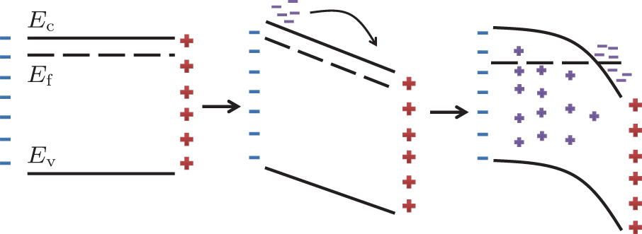
Fig. 3.3 Energy band of freestanding n-doped layer of AlGaN (left), the same layer used as a dielectric for a planar capacitor connected to a voltage source (middle), resulting curved energy band after transportation of free electrons leaving fixed positive charges on the negative electrode of the AlGaN capacitor (right).
Once taking to consideration the connection to GaN layer a fascinating thing will happen. Because the fermi level of GaN is lower of than of AlGaN, accumulated electrons will flow from the lower AlGaN layer to the top of GaN layer forming the resulting 2Deg (Fig.3.4). This process of growing 2Deg will stop when the Fermi levels of both materials will align with each other.
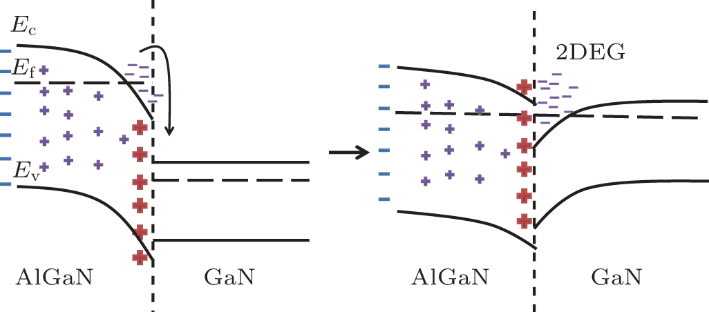
Fig. 3.4 Energy band of an n-doped AlGaN connecting to GaN showing different Fermi layers and electron flow to the GaN material (left), whole energy band of an n-doped AlGaN/GaN heterostructure after equalizing of Fermi levels showing the resulting 2Deg (right).
In real world we don’t need an n-doped AlGaN in order to create 2Deg. With intrinsic AlGaN the situation is different because of few or even no free electrons present in the material. Because of this fact the former method produce many issues, one of little or no electron transport resulting in almost no energy band bending although the tilting remains. Secondly, it can happen that the Fermi level of GaN could be higher than of AlGaN resulting in very few or no electron flow in to the GaN. And because of that no 2Deg should form. But in reality this is not the case.(2)
__________________
| (1) |
S. M. Sze , Physics of Semiconductor Devices, John Wiley & Sons, Inc. (1981) |
| (2) |
He Xiao-Guang, Zhao De-Gang, Jiang De-Sheng, Formation of two-dimensional electron gas at AlGaN/GaN heterostructure and the derivation of its sheet density expression, Chinese Physics B, 2015, 24(6): 067301 [online] |
 3 HEMT basic
3.2 Properties of the 2DEG
.
HEMTs unlike MOSFETs incorporates a so called 2DEG as the conducting channel. This 2DEG is formed at the heterojunction of the semiconductor structure and is always present as described in previous chapter. The key factor of the 2Deg or two dimensional electron gas is in its spatial confinement in the third dimension constraining electrons to move freely only in two dimension consisting only of conducting electrons which are distant from their parent atoms because of polarization effects in the structure.(1) Electrons can thus travel several micrometers before colliding into lattice of the semiconductor where the 2DEG is formed (Fig. 3.5). This collision-free environment in combination with low effective mass of electrons gives an extremely high mobility system (sometimes called “hot” electrons), which can be applied in fast electronic devices. Especially at low temperatures the mobility can be in orders of 1 000 000 cm2/Vs. This makes possible for 2Deg to have superior material properties such as high break-down electric field (5 MV/cm), high thermal conductivity (1.3 Wcm-1C-1), high peak velocity (>3x107cm-1s), high saturation velocity (>1.5x107cm-1s), and high sheet charge density (1x1013cm-2).(2)
Fig. 3.5 Electron movement in bulk and hetero structure (click to run)
__________________
| (1) |
B. J. Kelley, B. C. Dodrill, J. R. Lindemuth, G. Du, J.R. Meyer, L. Faraone, Electronic Transport Characterization of HEMT Structures, Solid State Technology 43.12 (2000): 130-134. [online] |
| (2) |
T. R. Lenka, A. K. Panda, Characteristics Study of 2DEG Transport Properties of AlGaN/GaN and AlGaAs/GaAs-based HEMT, Physics and Technology of Semiconductor 45 (5), 2011, [online] |
3 HEMT basic 
3.4 HEMT operation
.
A high electron mobility transistor (HEMT) is a kind of a field effect transistor where the current flow between two ohmic contacts, source and drain, is controlled by a third contact, the gate which may be a Schottky barrier contact in most cases.(1) Usually a field effect transistors channel is formed by a doped region as is generally the case for well known metal oxid semiconductor field effect transistor - MOSFET. Instead of that, HEMT incorporates a junction between two different semiconductor materials (i.e. a heterojunction) as the channel. The current is controlled in a way, that the transistor channel is normally open without gate biased (Fig. 3.6) .
HEMT advantages:
- High speed
- High gain
- Low noise
- High power density
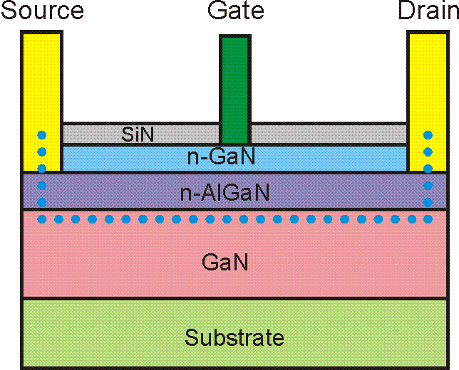
Fig. 3.6 HEMT operation
__________________
| (1) |
Helmut Brech, The Principles of a HEMT, [online] 1998, [cit. 2015-10-10] |
 3 HEMT basic
3.5 Types of HEMTs
.
III-V compound semiconductors are mainly used in HEMT’s as heterojunction materials for channel formation as shown in Fig. 3.7. The name high electron mobility transistor is derived from its high electron mobility nature which is a result of a quantum well (a special kind of potential well) near the hetero interface. In this well the conduction channel is a two dimensional electron gas (2DEG) instead of a three dimensional structure like in conventional FETs. As a result, it has significantly less Coulomb scattering, resulting in a very high mobility device structure.
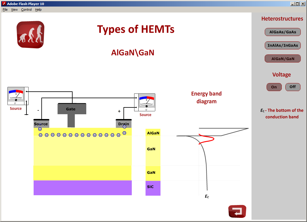
Fig. 3.7 Types of commonly used HEMTs (click to run)
Ideally, the two different materials used for a heterojunction would have the same lattice constant (spacing between the atoms). In practice, e.g. AlGaAs on GaAs, the lattice constants are typically slightly different, resulting in crystal defects. As an analogy, imagine pushing together two plastic combs with a slightly different spacing. At regular intervals, you'll see two teeth clump together. In semiconductors, these discontinuities form deep-level traps, and greatly reduce device performance.
A HEMT where this rule is violated is called a pseudomorphic HEMT or pHEMT. This is achieved by using an extremely thin layer of one of the materials – so thin that the crystal lattice simply stretches to fit the other material. This technique allows the construction of transistors with larger bandgap differences than otherwise possible, giving them better performance.
Another way to use materials of different lattice constants is to place a buffer layer between them. This is done in the metamorphic HEMT or mHEMT, an advancement of the pHEMT. The buffer layer is made of AlInAs, with the indium concentration graded so that it can match the lattice constant of both the GaAs substrate and the GaInAs channel. This brings the advantage that practically any Indium concentration in the channel can be realized, so the devices can be optimized for different applications (low indium concentration provides low noise; high indium concentration gives high gain).
In contrast to a modulation-doped HEMT, an induced HEMT provides the flexibility to tune different electron densities with a top gate, since the charge carriers are "induced" to the 2DEG plane rather than created by dopants. The absence of a doped layer enhances the electron mobility significantly when compared to their modulation-doped counterparts. This level of cleanliness provides opportunities to perform research into the field of Quantum Billiard for quantum chaos studies, or applications in ultra stable and ultra sensitive electronic devices.
 4 Electrical properties of HEMT
.
The HEMT theory is one thing, but the electrical properties show the real power of these devices. In this chapter are described direct current (DC) characteristics, which show the operation performance in fixed voltage biases, radio frequency (RF) performance, showing frequency limitations and high power performance, showing the electric power limitations. On Fig. 4.1 is depicted a symbol used for HEMT in schematics.
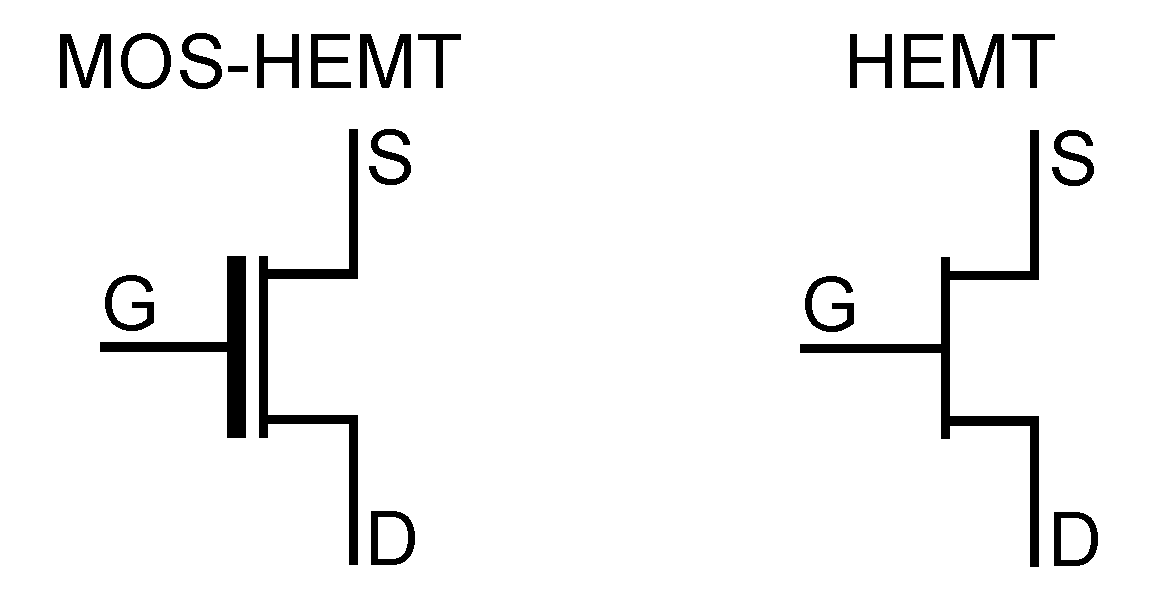
Fig. 4.1 HEMT symbols used in schematics for MOS-HEMT (left) and HEMT (right) with Schottky gate contact
 4 Electrical properties of HEMT
4.1 DC characteristics of HEMTs
.
HEMT, altrought different to a conventional MOSFET in terms of operation, is still a field effect transistor. Thus as a transistor it was developed in order to control large currents using small driving signals. HEMTs have a high potential especially in the high power and high frequency applications. To characterise the DC properties of a transistor a series of graphs is used, among which the I-V (current-voltage) characteristics called output and transfer characteristics are most known.(1)
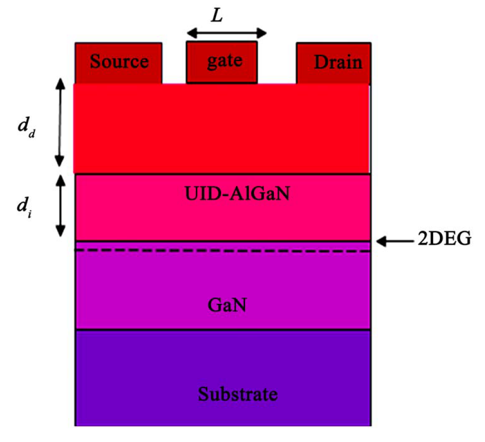
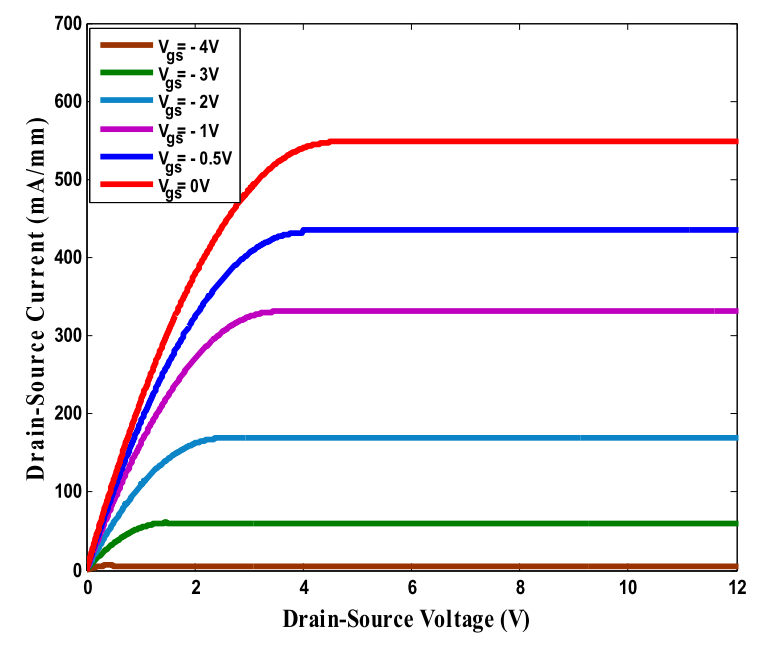
Fig. 4.2 Structure for HEMT simulation (left) and theoretical ideal characteristics Ids-Vds for an AlGaN/GaN HEMT at different gate Voltage (right)(2)
HEMT primarily works in depletion mode, i.e. current flows through the device even with no gate drive voltage. Voltage which has to be applied on the gate electrode in order to stop the current flow is called the pitch off voltage Vp. The best way to understand the HEMT electrical behavior is to develop a theorethical model and simulate the I-V characteristics. Figure 4.2 (left) shows the cross-sectional view of an AlGaN/GaN HEMT used for the simulation. The layer sequence is, from top to bottom, metal/n-AlGaN/undoped-AlGaN/undoped-GaN with a 2-DEG formed at the unintentionally doped (UID)-AlGaN/GaN interface. Figure 4.2 (right) shows the output Current-Voltage characteristics for different gate voltage Vgs ranging from −4 V to 0 V where -4 V is pitch off voltage Vp. For better understanding of this characteristics it is good to know the HEMT operation principle described in chapter 3.3. These characteristics correspond to an ideal HEMT structure, i.e. without considering the anomalies that may be present in this type of component. It appears clearly that the saturated drain current increases when increasing gate voltage.(2)
Fig. 4.3 HEMT DC characteristics (click to run)
A transfer characteristics shown on Fig. 4.3. displays the relation between gate voltage and drain current with a constant drain-source voltage Vds. To run the interactive animation click on the figure.
__________________
| (1) |
Anders Lundskog, Characterization of advanced AlGaN HEMT structures, Master thesis, 2007, [online] |
| (2) |
M. Charfeddine, H. Belmabrouk, M. A. Zaidi, H. Maaref, 2-D Theoretical Model for Current–Voltage Characteristics in AlGaN/GaN HEMT’s, Journal of Modern Physics, Vol.3 No.8, 2012, [online] |
 4 Electrical properties of HEMT
4.2 RF performance
.
To study dynamic characteristics it is needed to demonstrate a simulation of an appropriated and recessed n-GaN/AlxGa1-xN/GaN HEMT which schematic cross section is shown on figure left. Aluminum content equal to 10% in AlxGa1-xN donor layer, the gate-source spacing equal to 0.35µm, and the gate length equal to 50nm was set. The cap-layer is n-doped with a concentration equal to 5×1021cm-3, and the donor layer is n-doped with a concentration equal to 2×1020cm-3. All other layers are nonintentionally doped.
At high frequencies, the HEMTs are characterized by two important parameters: the cut-off frequency fT for which the modulus of the current gain is equal to 1 (0dB), and the maximum oscillation frequency fmax for which the unilateral power gain is equal to 1 (0dB). We calculate these two frequencies at room temperature; results are given respectively in Figs. 4.4 a) and b). At room temperature, the simulated cut-off frequency fT of about 331 GHz, and a maximum oscillation frequency fmax of about 1.1 THz which is a very promissing result for high frequency applications.(1)
Fig. 4.4 Evolution of the a) current gain as a function of frequency b) power gain as a function of frequency(1)
__________________
| (1) |
A. Hamdoune, M. Abdelmoumene, A. Hamroun, Static and Dynamic Characteristics of an Appropriated and Recessed n-GaN/AlGaN/GaN HEMT, World Academy of Science, Engineering and Technology International Journal of Electrical, Computer, Energetic, Electronic and Communication Engineering Vol:7, No:1, 2013, [online] |
 4 Electrical properties of HEMT
4.3 High power performance
.
Wide bandgap semiconductors show great promise for advancing the state-of-the-art for high power microwave electronic devices. Recent improvements in the growth of wide bandgap semiconductor materials, such as SiC and the GaN-based alloys, provide the opportunity to design and fabricate microwave transistors that demonstrate performance previously available only from microwave tubes. The most promising electronic devices for fabrication in wide bandgap semiconductors for these applications are MESFETs fabricated from 4H-SiC and heterojunction FETs (called HEMTs) fabricated using the AlGaN–GaN heterojunction. The theoretically predicted RF performance for an X-Band class A amplifier frequency of a 4H-SiC MESFET is shown in Fig. 4.5 left.(1) The theoretical predictions indicate that 4H-SiC MESFETs can produce RF output power on the order of 4–6 W/mm and should produce useful RF power through X-Band. The theoretical predictions are in excellent agreement with measured data, and the pre-dicted RF output power is experimentally obtained.(2)(3)
The structure for an AlGaN–GaN HFET is shown in figure on the left. The heterojunction is characterized with a 2DEG that has very high sheet charge density on the order of nss~1013cm-2. The high sheet charge density helps to produce high current capability for the HEMT. The wide bandgap semiconductors also permit high bias voltage to be applied with a drain bias of Vds=40 V these HEMTs are predicted to produce RF output power on the order of 10–12 W/mm of gate periphery.(1) RF output power greater than 10 W/mm has been obtained experimentally.(4) Recently, field-plates consisting of an extension of the gate metal to the region between the gate and drain(5), have been used to suppress gate breakdown, and these devices permit high bias voltages to be applied. Field-plate HEMTs have been biased as high as Vds=120 V, and these devices produce RF output power greater than 30 W/mm.(5)
Nitride-based HEMTs should be useful through Ka-Band, as shown in the predicted RF performance in Fig. 4.5 left, and should operate potentially well into the millimeter-wave region. Simulations indicate that these devices may provide good RF output power at frequencies as high as 100 GHz, as shown in Fig. 4.5 right. The Class A amplifier shown in Fig. 4.5 right is biased with Vds=30 V and produces RF output power of 400 mW with 17% power-added efficiency and 5 dB linear gain. Total amplifier RF output could be increased by power combining technology. Through X-band the RF power capability of the nitride-based HEMTs compares very favorably with the 1–1.5 W/mm RF power available from GaAs MESFETs and GaAs- and InP-based HEMTs.(1)
Fig. 4.5 Simulated RF performance for a 1-mm gate width AlGaN–GaN HEMT class A amplifier (left) and predicted RF performance for an AlGaN–GaN HEMT class amplifier at 100 GHz, V = 30 V, class A (right)(1)
__________________
| (1) |
Robert J. Trew, High-Frequency Solid-State Electronic Devices, IEEE TRANSACTIONS ON ELECTRON DEVICES, VOL. 52, NO. 5, MAY 2005, [online] |
| (2) |
H. G. Henry, S-band operation of SiC power MESFET with 20 W(4.4 W/mm) output power and 60% PAE, IEEE Trans. Electron Devices, vol. 51, no. 6, pp. 839–845, Jun. 2004, [online] |
| (3) |
R. C. Clarke and J. W. Palmour, SiC microwave power technologies, Proc. IEEE, vol. 90, no. 6, pp. 987–992, Jun. 2002, [online] |
| (4) |
Y.-F. Wu, A. Saxler, M. Moore, R. P. Smith, S. Sheppard, P. M. Chavarkar, T. Wisleder, U. K. Mishra, and P. Parikh, 30-W/mm Gan HEMTs by field plate optimization, IEEE Electron Device Lett., vol. 25, no. 11, pp. 117–119, Nov. 2004, [online] |
| (5) |
U. K. Mishra, P. Parikh, and Y.-F. Wu, AlGaN/GaN HEMTs-an overview of device operation and applications, Proc. IEEE, vol. 90, no. 6, pp. 1022–1031, Jun. 2002, [online] |
 5 HEMT design and fabrication
.
The design and fabrication is coming out of the used material properties and functionality. In this chapter are ultimate facts about HEMT construction, materials, fabrication layout and growth chalengest described. Together with simulations it makes the technology and fabrication whole.
 5 HEMT design and fabrication
5.1 HEMT construction
.
In order to increase RF output power it is necessary to decrease the leakage current resulting from the tunnelling of electrons from the gate metal to the surface of the semiconductor. This can be accomplished by decreasing the magnitude of the electric field at the gate edge.
The use of field plate technology has long been recognized as a useful technique for suppression of voltage at critical locations within a semiconductor device. Schematic figure of GaN/AlGaN HEMT without and with fieldplate is depicted in Fig. 5.1. The field plate consists of an additional metal layer located over the gate metal (Fig. 5.1 right) and extending into the region between the gate and drain. The gate metal provides an electric field termination layer that reduces the magnitude of the field at the gate edge, thereby suppressing the gate leakage current.
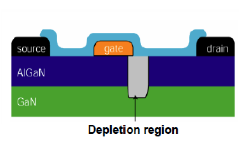
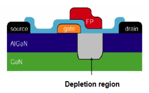
Fig. 5.1 Schematic figure of GaN/AlGaN HEMT without (left) and with (right) fieldplate.
The use of field-plate technology permits high drain bias voltages to be applied, thereby producing improvements in RF output power. In fact, the degree of gate leakage suppression is sufficient to permit drain bias on the order of V DS =100-120 V to be applied. This allows high RF output power to be generated. However, field plates also introduce additional capacitance and reduce the transconductance of the transistor. Therefore a degradation in frequency performance occurs. For this reason, a minimum field-plate length should be employed.(1)
The current in convential HEMT is controlled in a way, that the transistor channel is normally open without gate biased . This makes the implementation of HEMT in electrical circuit very complicated and therefore there are atempts to fabricate a normally off transistor with the same advantages as convential HEMT.
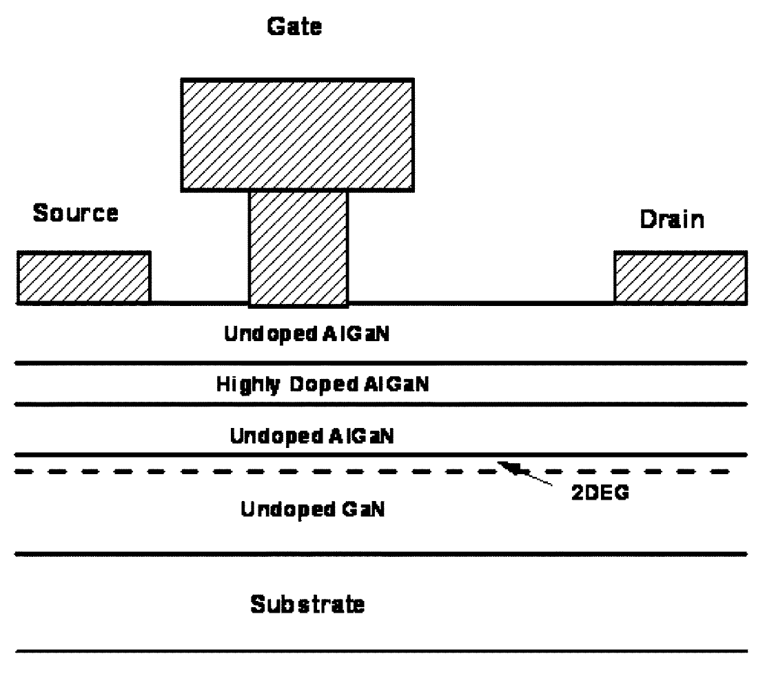
The approach using recessed MIS-gate HEMT designated to be used for power applications is shown on Fig. 5.2 top-left. The epitaxial layers grown on a silicon substrate consist of a buffer layer for relaxing the strain between the substrate and GaN-based layers, an 800-nm-thick AlGaN buffer layer, a 40 nm thick GaN channel layer, 34/1 nm thick AlGaN/AlN barrier layers, and a 1-nm-thick GaN cap layer. The layers of the recessed region were etched by SiCl4/Cl2 using inductively coupled plasma. A maximum field-effect mobility of 120 cm2/Vs and a maximum drain current over 200 mA/mm were attained.(2)
The aproach using fluorine ion implantation of AlGaN barrier designated to be used for RF applications is shown on Fig. 5.2. top-right. Device isolation was carried out by mesa etching with chlorine-based plasma in an inductively coupled plasma reactive ion etching (ICP-RIE) system. After the T-gate windows were opened, the sample was implanted by CF4 plasma in an reactive ion etching (RIE) system with an RF plasma power of 150 W for 150 s. The device exhibits a thresh old voltage of +0.2 V, a saturation drain current density of 735 mA/mm, current-gain cutoff frequency (fT) is closed to 40 GHz, and the power-gain cutoff frequency (fmax) presents more than 90-GHz.(3)
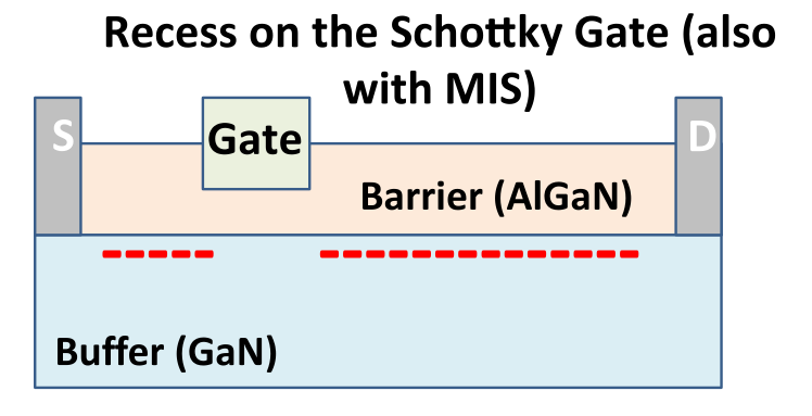
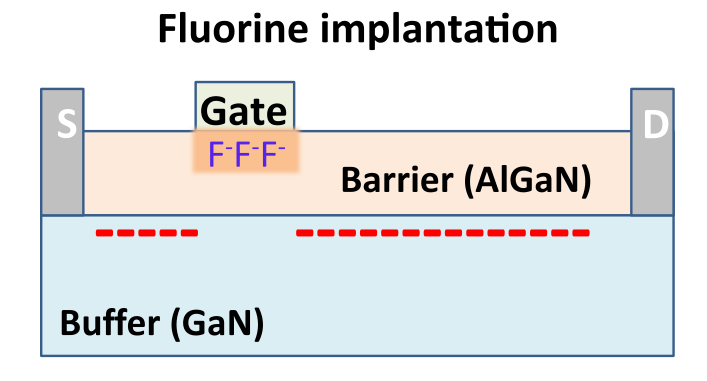
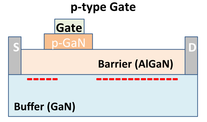
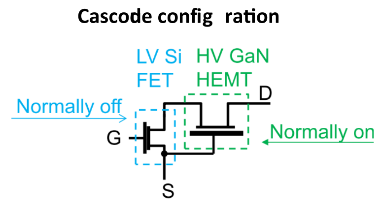
Fig. 5.2 Schematic figures of GaN/AlGaN HEMTs with normally off state using recess on the Schottky gate (top-left), fluorine ion implementation (top-right), p-type gate (bottom-left) and cascode circuit configuration (bottom-right)
The aproach using gate injection transistor (p-gate) designated to be used for switching applications is shown on Fig. 5.2. bottom-right. The gate injection transistor (GIT) utilizes hole injection from the p-type gate to the 2DEG region bringing out the conductivity modulation as observed in insulated-gate bipolar transistors (IGBTs). This new concept enables both normally-off operation and high current driving capability by applying high positive gate voltage with low gate current. A p-AlGaN/i-AlGaN/GaN heteroepitaxial structure for the GIT is grown on a Si substrate with buffer layers consisting of the GaN/AlN multilayers on top of the AlGaN/AlN initial layers. The resulting RON·A and the breakdown voltage are 2.6 mΩ·cm2 and 800 V, respectively. The GIT achieves a high drain current of 200 mA/mm with the threshold voltage of 1.0 V.(4)
In order to achieve a simple normally off state HEMT we can use two separate devices forming a circuit called cascode circuit shown on Fig. 5.2 bottom right. The circuit consist of a low voltage normally of Si field effect transistor (FET) interconnected with normally on GaN HEMT. In this configuration the FET controls the HEMT's gate- source voltage for normally off operation and keeping high voltage capability of HEMT in the same time .
__________________
| (1) |
Trew, R.J., Wide bandgap transistor amplifiers for improved performance microwave power and radar applications, 15th International Conference on Microwaves, Radar and Wireless Communications, MIKON - 2004, [online] |
| (2) |
T. Oka, T. Nozawa, AlGaN/GaN Recessed MIS-Gate HFET With High-Threshold-Voltage Normally-Off Operation for Power Electronics Applications, IEEE ELECTRON DEVICE LETTERS, VOL. 29, NO. 7, JULY 2008, [online] |
| (3) |
Z. H. Feng , R. Zhou, S. Y. Xie, J. Y. Yin, J. X. Fang, B. Liu, W. Zhou, Kevin J. Chen, S. J. Cai, 18-GHz 3.65-W/mm Enhancement-Mode AlGaN/GaN HFET Using Fluorine Plasma Ion Implantation, IEEE Electron Device Letters, Volume:31, Issue: 12, pp. 1386-1388, October 2010, [online] |
| (4) |
Y. Uemoto, M. Hikita, H. Ueno, H. Matsuo, H. Ishida, M. Yanagihara, T. Ueda, T. Tanaka, D. Ueda, Gate Injection Transistor (GIT)—A Normally-Off AlGaN/GaN Power Transistor Using Conductivity Modulation, IEEE Transactions on Electron Devices, Volume:54, Issue:12, pp. 3393-3399, Dec. 2007, [online] |
 5 HEMT design and fabrication
5.2 Materials perspective
.
III-N material based devices have gained more attention, due to their good thermal conductivity, high breakdown field and high saturation velocities (see Tab. 5.1). But GaN based devices are facing many problems because bulk GaN substrates are not currently available. To improve material quality and be able to dissipate heat in high-power devices the structures are hetero-epitaxially grown on foreign substrate. Presently, GaN devices are fabricated on sapphire (in spite of a significant lattice mismatch), Si(111) (which shows better thermal conductivity but larger lattice mismatches than sapphire), or SiC (with better matches, excellent thermal conductivity, but still highly defective and at prohibitive price).(1)
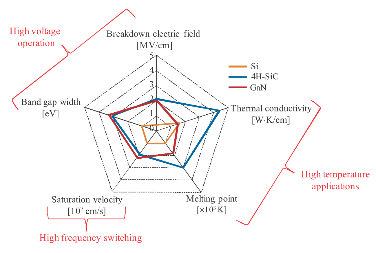
Fig. 5.3 Summary of Si, SiC, and GaN relevant material properties.(3)
Even when GaN substrates become available, they will not provide as much heat removal capability as SiC substrates (Fig. 5.3). This suggests that the most efficiently cooled GaN HEMTs will be those grown on SiC and that the defects, which arise from the heteroepitaxy of GaN on SiC, must be reduced or their influence nullifie.(2)
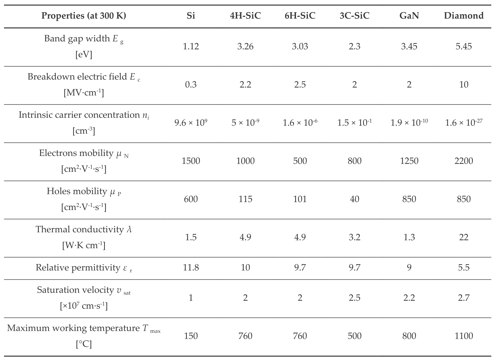
Tab. 5.1 Comparison between intrinsic properties of Si and WBG semiconductor materials.(3)
__________________
| (1) |
F. Calle, T. Palacios, E. Monroy, J. Grajal, M. Verdú, Z. Bougrioua, I. Moerman, AlGaN/GaN HEMTS: material, processing, and characterization, Journal of Materials Science: Materials in Electronics, Volume 14, Issue 5, pp 271-277, May 2003, [online] |
| (2) |
Daniel D. Koleske, Andrew A. Allerman, S. R. Kurtz, Stephen R. Lee, Alan F. Wright, Carleton H. Seager, Nancy A. Missert, Albert G. Baca, Ronald D. Briggs, Phil F. Marsh, Chris P. Tigges, Randy J. Shul, David M. Follstaedt, and Paula P. Provencio, Materials Physics and Device Development for Improved Efficiency of GaN HEMT High Power Amplifiers., Sandia National Laboratories , December 2005, [online] |
| (3) |
O. Deblecker, Z. De Grève and C. Versèle, Comparative Study of Optimally Designed DC-DC Converters with SiC and Si Power Devices, Advanced Silicon Carbide Devices and Processing, 2015, [online] |
 5 HEMT design and fabrication
5.3 Transistor fabrication layout
.
The following sections will outline the processes required to take an epitaxially grown wafer through to the completed working device stage. Fig. 5.4 shows the process flow for photolithography and metallisation and should be referred to when reading the following sections.
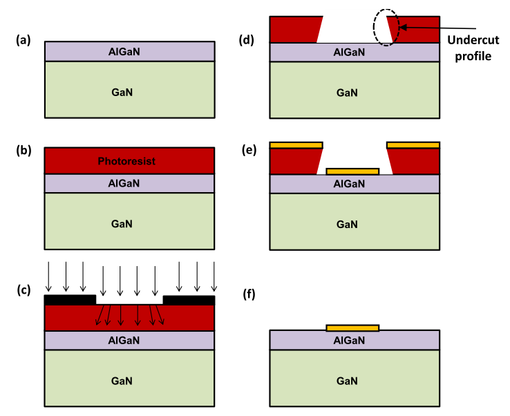
Fig. 5.4 Device process (a) Sample has been cleaned and is ready to be processed (b) Photoresist is spun onto sample (c) Sample has been soaked in developer solution and is now being subjected to UV light. The black boxes on top of the photoresist indicate the mask plate in contact with the sample, protecting areas which do no require to be patterned (d) Photoresist is developed and shows an undercut profile which will benefit the metal lift-off process (e) The sample is then metallised in the electron beam evaporator (f) Finally the sample is immersed in warm acetone to remove the photoresist and leave behind only the metal which was evaporated directly onto the material.
The layout of a typical RF transistor unit cell for research purposes consists of two gate fingers and is shown in Fig. 5.5 (when implemented for amplifiers etc. the number of fingers will increase to increase the output current/power). When fabricating many RF devices on the same sample of material, a mesa isolation step is required to electrically isolate them from one another on the sample.(1)
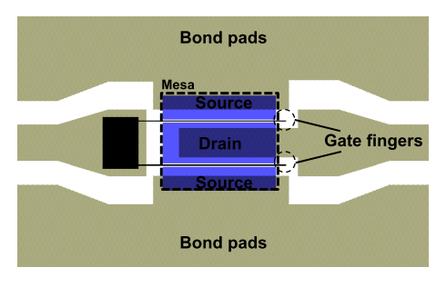
Fig. 5.5 Typical layout of unit cell of RF device which has two gate fingers.
__________________
| (1) |
Douglas James Macfarlane, Design and fabrication of AlGaN/GaN HEMTs with high breakdown voltages, PhD Thesis, School of Engineering, University of Glasgow, 2014, [online] |
 5 HEMT design and fabrication
5.4 Growth challenges
.
Several growth techniques are used to fabricate AlGaN/GaN HEMTs. Among all the most used are metal organic vapor phaze epitaxy (MOCVD) which provides best material properties and molecular beam epitaxy (MBE) with the advantage of improved interface quality. Whatever the substrate or the technique is being used, material growth is a key challenge for the device operation. (1)
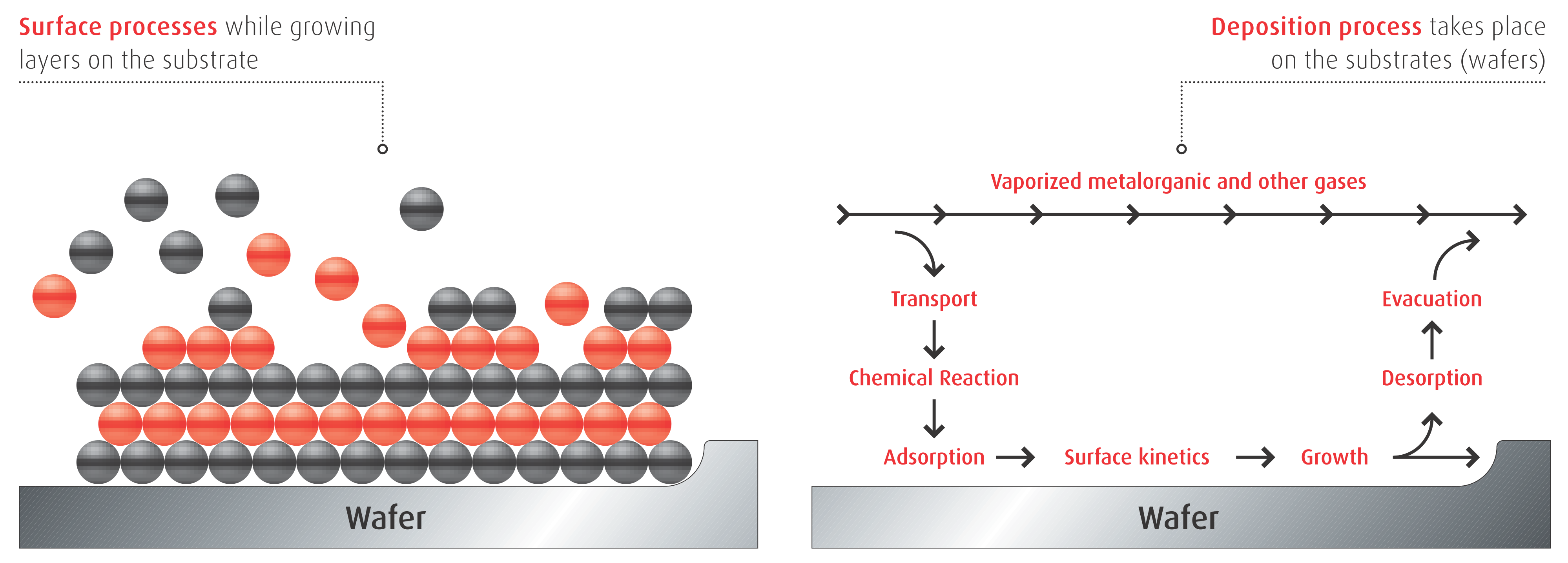
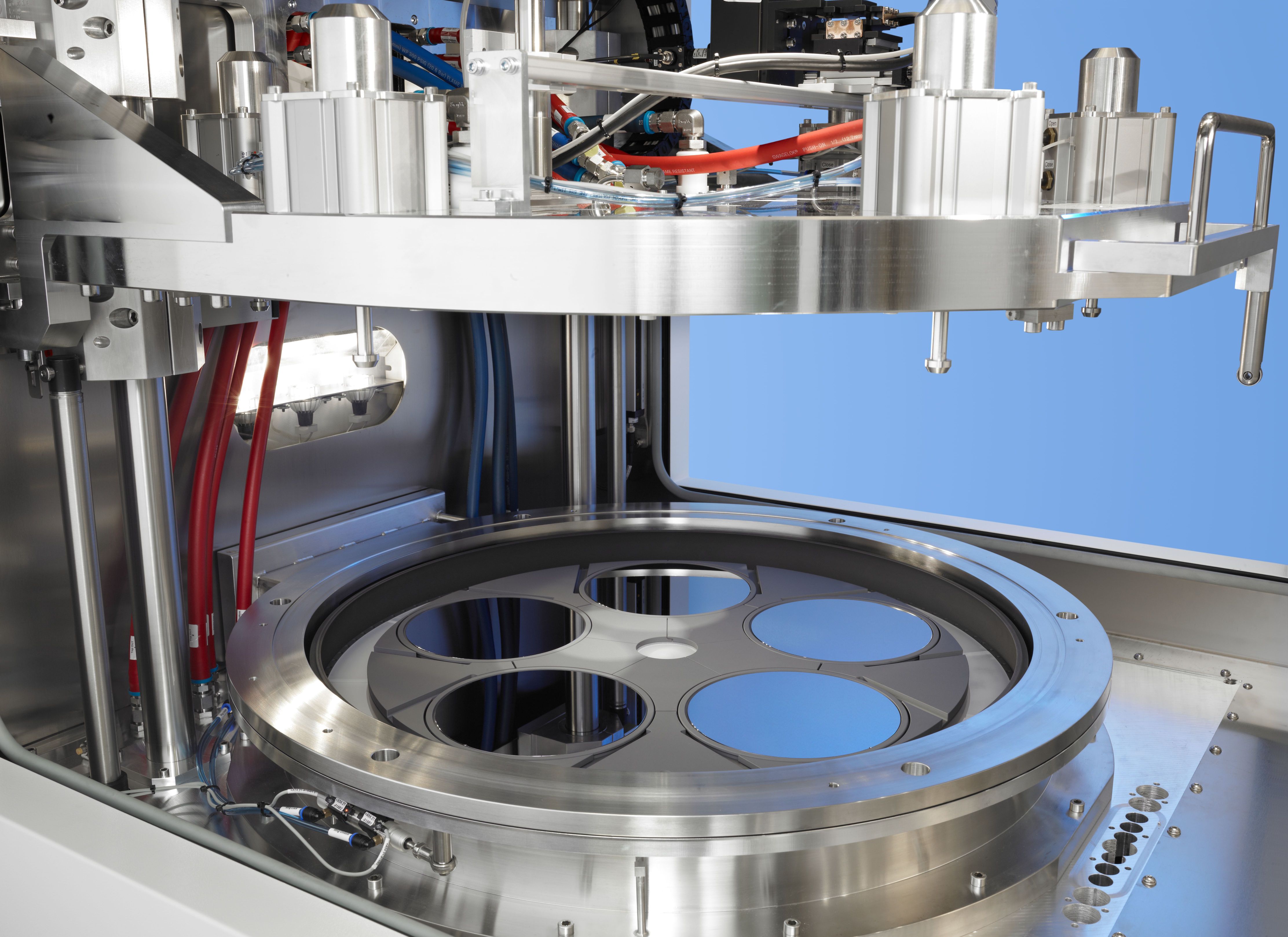
Fig. 5.6 MOCVD epitaxy principle and AIX G5+ reactor chamber(2)
MOCVD has been the most commonly used technique for developing GaN based epilayers and is carried out at temperatures in excess of 1000◦C and involves gaseous reactants (such as trimethylgallium and NH3) passing over a heated substrate which react to form a condensed layer or film on the substrate. Growth rates are typically between 1 - 2 µm per hour. MBE on the other hand, is a slower process with growth rates typically between 0.5 - 1 µm per hour and is carried out at lower temperatures compared to MOCVD (500 - 900◦C). MBE uses solid Ga and Al sources along with NH3 and occurs via reactions between thermal-energy molecular, atomic, or ionised beams of the constituent elements on a heated substrate in an ultra-high vacuum.(3)
The major technical issues associated with GaN HEMT technology are the presence of defects including traps and dislocations, thermal management of the operating devices, dislocations near the active regions, and growth and device fabrication reproducibility.
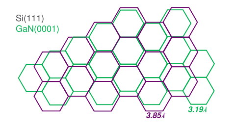
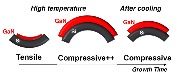
Fig. 5.7 Difficulties of growing GaN on Si because of lattice mismatch (left) and thermal expansion mismatch (right)(5)
Defects are introduced into the HEMT structure during the growth. The most common defects that occur in GaN are dislocations, impurities, and point defects. Dislocations originate in GaN at the hetero-interface partly due to the lattice mismatch between SiC and GaN and partly due to the discrete GaN grains, which form and ultimately coalesce on the SiC to form the film. Dislocations in GaN typically range from 10 8 to 10 10 cm -2 and this density is independent of growth technique. Impurities and point defects on the other hand are more strongly influenced by the reactor growth conditions. Each of these defects can adversely affect device performance by creating charge trapping centers and leakage pathways, which can ultimately lead to device failure and reliability issues.
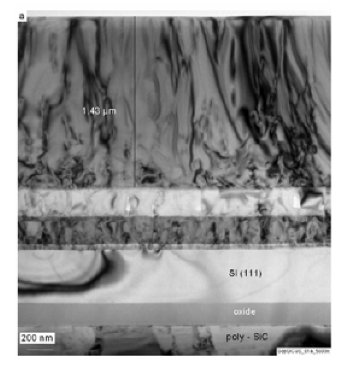
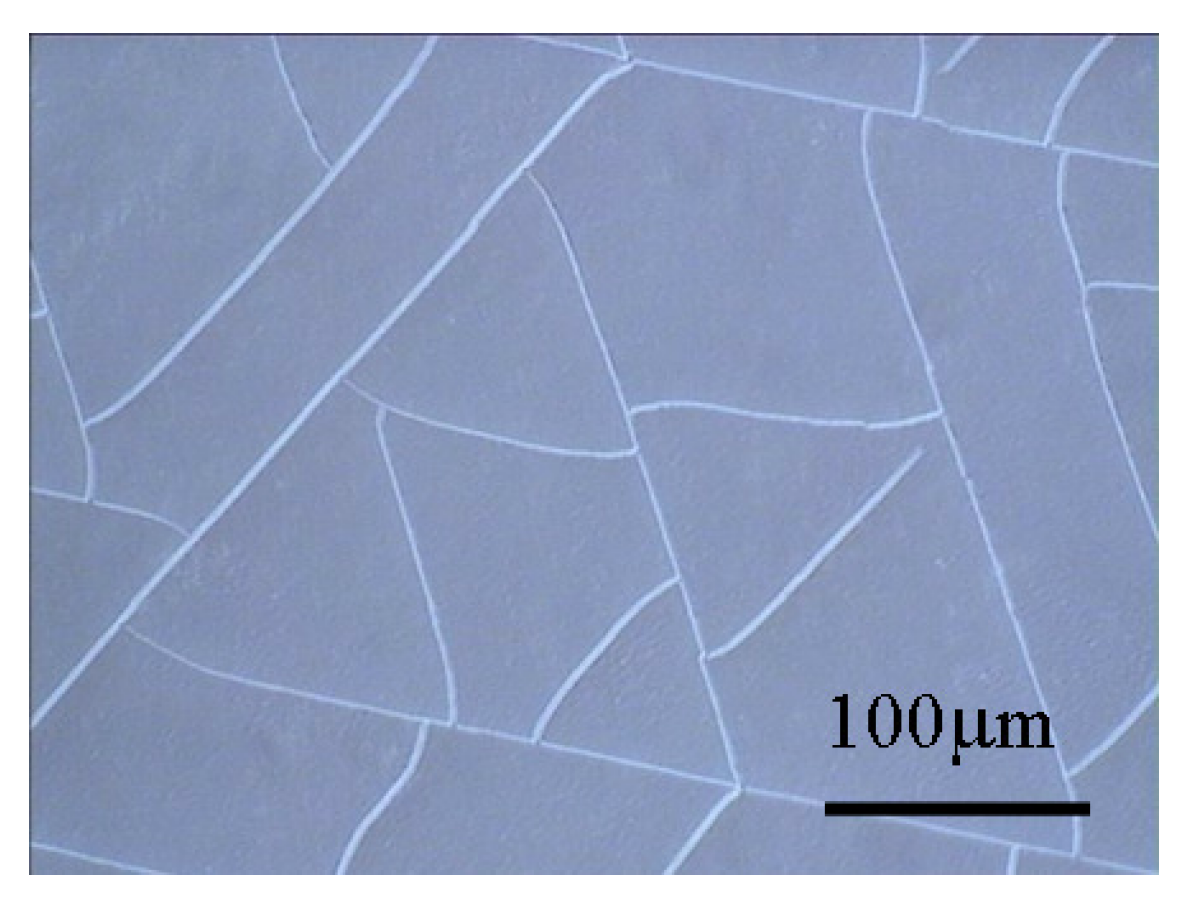
Fig. 5.8 Consequences of lattice mismatch leading to defects in the structure (left)(6) and thermal expansion mismatch leading to GaN layer cracking on a surface (right)(5)
Trapping type defects can dramatically limit frequency performance, especially in the GaN or AlGaN layers near the two dimensional electron gas (2-DEG). For a HEMT to work properly the GaN must be insulating enough such that current flows only through the 2-DEG and not in parallel through the bulk GaN. If on the other hand, the semi-insulating (SI) GaN is too resistive electron traps may be present in the GaN. Traps can also produce current collapse in HEMT devices, which is caused when hot electrons are injected into the insulating GaN region. Once trapped, the electrons cannot be thermally emitted because of the large bandgap. As a result the electrons effectively back gate the device, leading to reduced current flow in the 2-DEG. In addition to hot electron injection, cycling either the gate or drain voltage can cause transient reductions in the drain current. Traps are also likely present in the AlGaN and at surface of HEMTs. Traps may result from impurity, vacancy, or dislocation structures. Ultimately, these traps limit gain, linearity, power-added-efficiency, reproducibility, and reliability in GaN-based HEMT devices. To date, not been much progress has been made in solving these trap related issues that influence rf-dispersion.
Ideally, bulk GaN substrates could reduce or eliminate the influence of trapping type defects on HEMT performance, especially traps associated with dislocations. However, during operation junction temperatures of HEMTs are greater than 200 ºC, which can lead to device breakdown and loss of linearity. This suggests that active cooling of the devices is potentially as important as reducing the influence of traps. Because SiC has a high thermal conductivity and is closely lattice matched GaN (3.5% difference) and AlN (< 1% difference), SiC is the best substrate for GaN HEMTs. To date the GaN HEMTs with the best power performance have been grown on SiC.
The main issue with GaN heteroepitaxy on SiC is that threading dislocations are formed in the GaN. 100 nm of AlN is first grown on the SiC to provide nucleation sites and enhance two dimensional growth of the GaN. Growth of the AlN layer generates primarily edge type dislocations resulting from the discrete granularity of the AlN film. These edge dislocations can then propagate through the GaN and AlGaN films. While these dislocations are benign to transport in the 2-DEG they can limit the maximum source-drain voltage and provide shorting pathways within the device. Additional misfit dislocations can be generated at the AlGaN/GaN interface, especially when the Al concentration exceeds 30%. Techniques to reduce dislocations, such as epitaxial lateral overgrowth (ELOG), have not been extensively studied for improving HEMT performance.
Finally, there are many issues associated with the growth and characterization GaN HEMTs on SiC that have not yet been identified or addressed. In general, the growth and theory of how semi-insulating (SI) GaN is produced on SiC is not well controlled or understood. Surprisingly, some researches in the field have suggested that the GaN grain structure may play a pivotal role in achieving SI GaN. If this is the case, then reproducible nucleation of the GaN to replicate the same grain structure is absolutely necessary. Understanding of the physics behind the operation of GaN HEMTs is also lacking. This is primarily because physics measurements of the HEMT material properties are difficult and models of HEMTs with traps, dislocations, and surface charge have not been developed. (4)
__________________
| (1) |
F. Calle, T. Palacios, E. Monroy, J. Grajal, M. Verdú, Z. Bougrioua, I. Moerman, AlGaN/GaN HEMTS: material, processing, and characterization, Journal of Materials Science: Materials in Electronics, Volume 14, Issue 5, pp 271-277, May 2003, [online] |
| (2) |
AIXTRON webpage, [online] |
| (3) |
Douglas James Macfarlane, Design and fabrication of AlGaN/GaN HEMTs with high breakdown voltages, PhD Thesis, School of Engineering, University of Glasgow, 2014, [online] |
| (4) |
Daniel D. Koleske, Andrew A. Allerman, S. R. Kurtz, Stephen R. Lee, Alan F. Wright, Carleton H. Seager, Nancy A. Missert, Albert G. Baca, Ronald D. Briggs, Phil F. Marsh, Chris P. Tigges, Randy J. Shul, David M. Follstaedt, and Paula P. Provencio, Materials Physics and Device Development for Improved Efficiency of GaN HEMT High Power Amplifiers., Sandia National Laboratories , December 2005, [online] |
| (5) |
Y. Saripalli, IEEE-ICEE 2014 |
| (6) |
T. J. Anderson, F. Ren, L. Voss, M. Hlad, B. P. Gila, S. J. Pearton, J.Kim, J. Lin, P. Bove, H. Lahreche, J. Thuret and R. Langer, AlGaN/GaN High Electron Mobility Transistors and Diodes Fabricated on Large Area Silicon on poly-SiC (SopSiC) Substrates for Lower Cost and Higher Yield , CS MANTECH Conference, May 14-17, 2007, [online] |
 5 HEMT design and fabrication
5.6 3D simulations
.
Multifinger HEMT devices with compact layout are required for high-power operation, however, self-heating induced thermal crosstalk between individual gate fingers becomes serious, which degrades device performance or results in irreversible damage. Therefore, thermal management is crucially important to the viability of power HEMTs.
Our proposed methodology for fast 3-D device electrothermal simulation is based on direct coupling between finite element method (FEM) thermal and circuit electrical simulation using mixed-mode setup(1) supported in Synopsys TCAD Sentaurus environment(2). The mixed-mode setup allows direct interconnection of a 3-D FEM thermal model of the whole system (semiconductor layers, package, printed circuit board (PCB) up to cooling assemblies), 3-D FEM electrical model of the metallization layers and an equivalent electrical temperature dependent circuit model of the HEMT (Fig. 5.9)(3).
This approach combines the speed and accuracy, and couples temperature and current density nonuniformity in structure and metallization layers. The 3-D FEM model of the structure based on the physical and geometrical description of all semiconductor and metallization layers corresponding to the real device is created in Synopsys device editor. The metallization layers are created by Synopsys layout editor, which allows viewing and editing the layouts in most of the industry-standard formats including GDSII.
The advantages of the proposed method are the relative simplicity of implementation, the speed of simulation and the capability of a full analysis of complex structures. The effects of structure design and fabrication parameters including semiconductor layers, metallization, package, and up to cooling assemblies are studied.
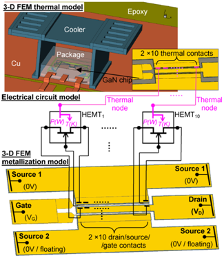
Fig. 5.9 Circuit diagram of the electrothermal mixed-mode simulation. Equivalent HEMT circuit model is connected to 3-D thermal model by the thermal nodes. Heat flux and temperature exchange is provided via thermal nodes. The current density distribution and the voltage drop on parasitic resistances are solved in 3-D electrical model of the metallization.
Fig. 5.10 a shows a comparison of the measured and simulated output characteristics for two different measurement setups. The first setup connects only Source 1 to the ground and only one gate finger is active. The second setup connects both sources to the ground and both gate fingers are active. The temperature interaction between the gate fingers for the second setup shows a drop of the output characteristics, which is caused by a higher structure temperature compared to the first setup (Fig. 5.10 c (Cross section A)). Moreover, there is an additional voltage drop due to the metal resistance caused by doubled current flowing through drain metallization layer (Fig. 5.10 b). Its main impact is in the linear region of the output characteristics. The proposed 3-D electrothermal simulation splits the structure along the gate into several parts, which allows analysis of the inhomogeneous distribution of temperature and of the electrical properties. The inhomogeneous distributions of temperature and current along the gate electrode are shown in Fig. 5.10 c (Cross section B). The lower temperature and higher current density at the HEMT edge segments are caused by more effective cooling of the structure edges compared with the central segment.
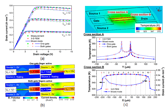
Fig. 5.10: (a) Comparison of measured and simulated output characteristics and (b) electrostatic potential and current density distribution in the metallization for one and both gate fingers active. For both gate fingers active is an additional voltage drop due to the metal resistance caused by doubled current flowing through drain metallization layer. (c) Temperature distribution of the HEMT for VDS = 15 V and VGS = 1 V (top). (Cross section A) Comparison of the temperatures across the gate electrodes for one and both gate fingers active. (Cross section B) Temperature and current distributions inside the HEMT structure along the gate electrode.
__________________
| (1) |
CHVÁLA, Aleš, DONOVAL, Daniel, ŠATKA, Alexande, MOLNÁR, Marián, MAREK, Juraj, PRÍBYTNÝ, Patrik, Advanced methodology for fast 3-D TCAD device/circuit electrothermal simulation and analysis of power HEMTs, IEEE Transactions on Electron Devices, Vol. 62, No. 3, pp. 828-834, 2015, [online] |
| (2) |
Synopsys, San Jose, CA, USA. (1986). Technology Computer-Aided Design, [online] |
| (3) |
CHVÁLA, Aleš, DONOVAL, Daniel, MOLNÁR, Marián, MAREK, Juraj, PRÍBYTNÝ, Patrik, Advanced methodology for fast 3-D TCAD electrothermal simulation of power HEMTs including package, SISPAD 2015 : International conference on simulation of semiconductor processes and devices, Washington DC, USA, September 9-11, Piscataway : IEEE, 2015, S. 116-119. ISBN 978-1-4673-7859-8, 2015, [online] |
 6 HEMT applications
.
The HEMT was originally developed for high speed applications. The technological advantages of GaN/AlGaN HEMT result from the combination of the wide-band gap of GaN and the availability of the AlGaN/GaN heterostructure where high voltage, high current and low on-resistance can be simultaneously achieved, resulting in high power-high efficiency operation. Furthermore, the wide-bandgap offers a rugged and reliable technology capable of high voltage-high temperature operation. This opens up several industrial, automotive and aircraft applications like power and high voltage rectifiers and converters. Some of the commercial and military markets that can be targeted by GaN are shown on Fig. 6.1.(1)
It was only when the first devices were fabricated that it was discovered they exhibited a very low noise figure. This is related to the nature of the two dimensional electron gas and the fact that there are less electron collisions. As a result of their noise performance they are widely used in low noise small signal amplifiers, power amplifiers, oscillators and mixers operating at frequencies up to 60 GHz and more and it is anticipated that ultimately devices will be widely available for frequencies up to about 100 GHz.
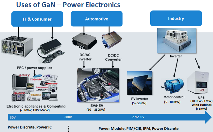
Fig. 6.1 Power electronics applications for GaN HEMTs (source: Yole)
In fact HEMT devices are used in a wide range of RF design applications including cellular telecommunications, Direct broadcast receivers - DBS, radar, radio astronomy, and any RF design application that requires a combination of low noise and very high frequency performance HEMTs are manufactured by many semiconductor device manufacturers around the globe. They may be in the form of discrete transistors, but nowadays they are more usually incorporated into integrated circuits. These Monolithic Microwave Integrated Circuit chips, or MMICs are widely used for RF design applications, and HEMT based MMICs are widely used to provide the required level of performance in many areas.(2)
 Fig. 6.1 RF applications for GaN HEMTs (click to run)
__________________
| (1) |
U. K. Mishra, P. Parikh, Yi-Feng Wu, AlGaN/GaN HEMTs-an overview of device operation and applications, Proceedings of the IEEE, Volume:90 Issue:6, 2002, [online] |
| (2) |
saniks, HEMT, [online] |
 6 HEMT applications
6.1 HEMTs in integrated microwave circuits
.
A Monolithic Microwave Integrated Circuit, or MMIC (sometimes pronounced "mimic"), is a type of integrated circuit (IC) device that operates at microwave frequencies (300 MHz to 300 GHz). These devices typically perform functions such as microwave mixing, power amplification, low-noise amplification, and high-frequency switching. Inputs and outputs on MMIC devices are frequently matched to a characteristic impedance of 50 ohms. This makes them easier to use, as cascading of MMICs does not then require an external matching network. Additionally, most microwave test equipment is designed to operate in a 50-ohm environment. Mini-Circuits' extensive selection of RF amplifiers offers many combinations of gain, noise figure, output power, and linearity in MMIC, surface mount, and connector packages.
Based on Cree GaN high electron mobility transistors (HEMTs), the new MMIC is built on a SiC substrate using a 0.25μm gate length fabrication process. GaN-on-SiC exhibits several superior properties compared to silicon (Si), gallium arsenide (GaAs), and GaN-on-Si, including higher breakdown voltage, saturated electron drift velocity, and thermal conductivity. GaN HEMTs also offer greater power density and wider bandwidths than Si, GaAs, and GaN-on-Si transistors (Fig. 6.3).
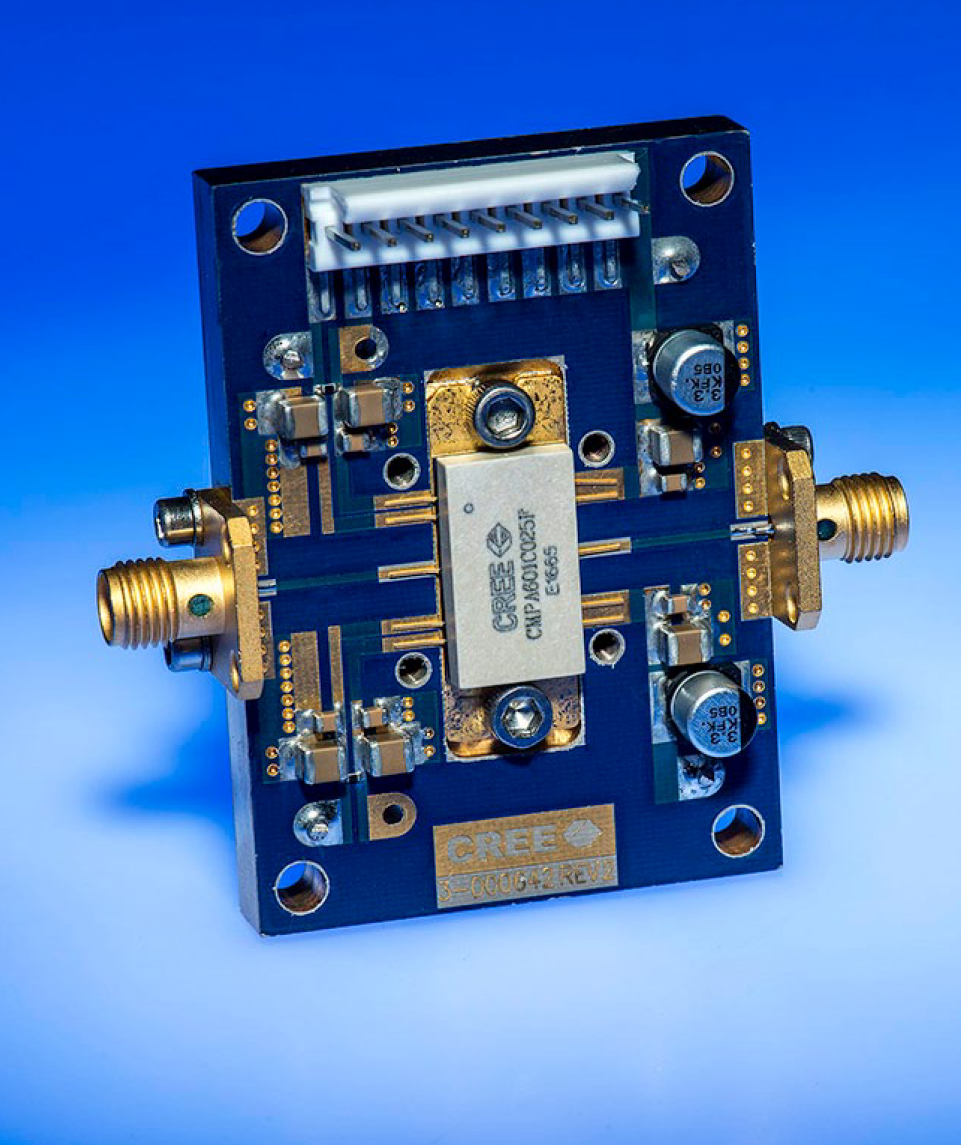
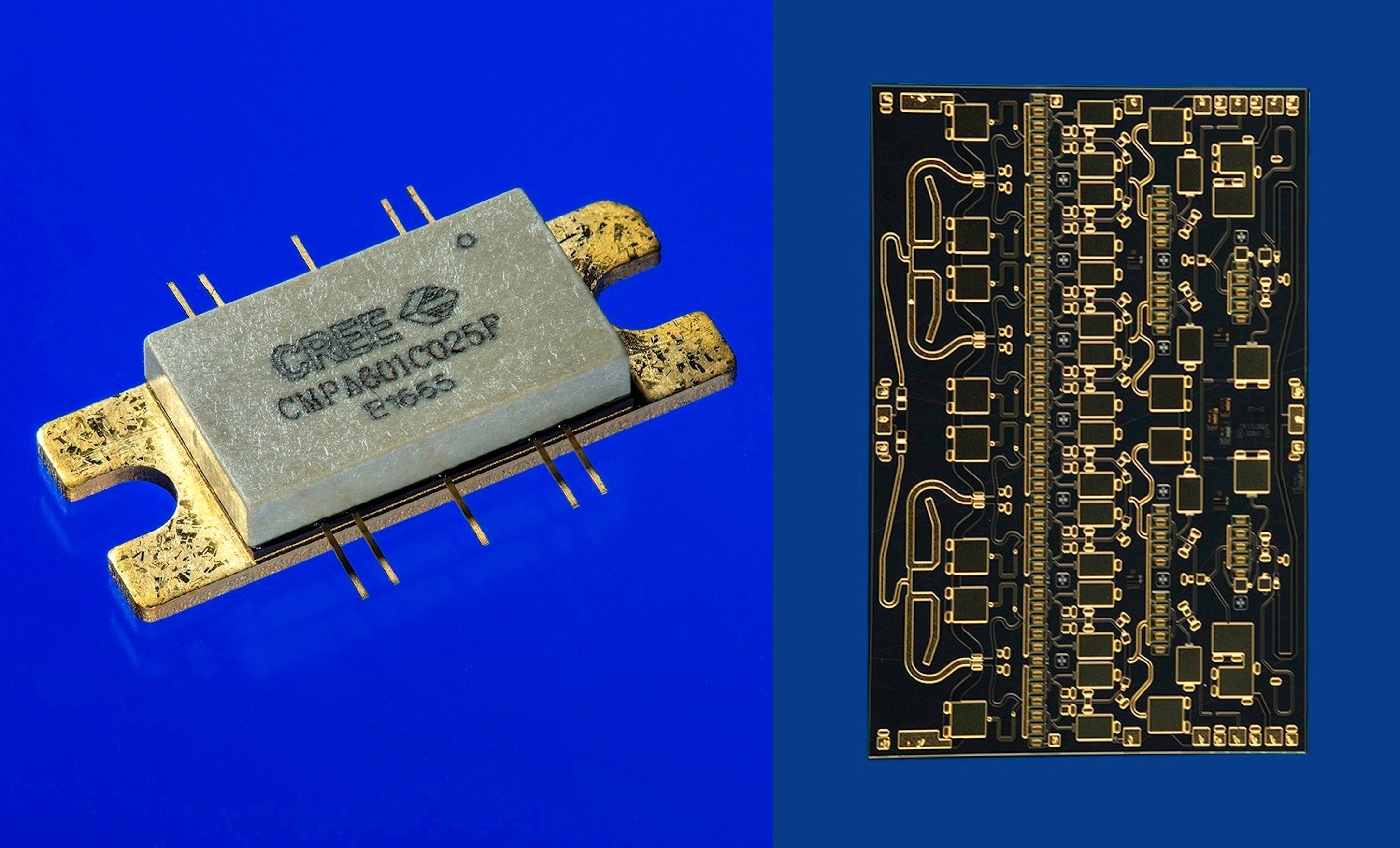
Fig. 6.3 GaN HEMT Monolithic Microwave Integrated Circuit (MMIC) amplifier (source: CREE)
 6 HEMT applications
6.2 HEMTs in integrated power circuits
.
Highly modern power transistors based on gallium nitride (GaN) enable power electronic switches to operate at much higher switching frequencies compared to those based on silicon (Si). An increased power density per volume and per weight, reduced costs, less material use and, in the case of a mobile system, increased system efficiency are among the advantages.
The scientist in Fraunhofer institute have develop a resonant DC/DC converter with GaN transistors (Fig. 6.4), which is to operate with switching frequencies well above 1 MHz and a nominal power of 3 kW. The simultaneous occurrence of extremely high switching frequencies and high transmitted power requires the use of special, innovative inductive components.
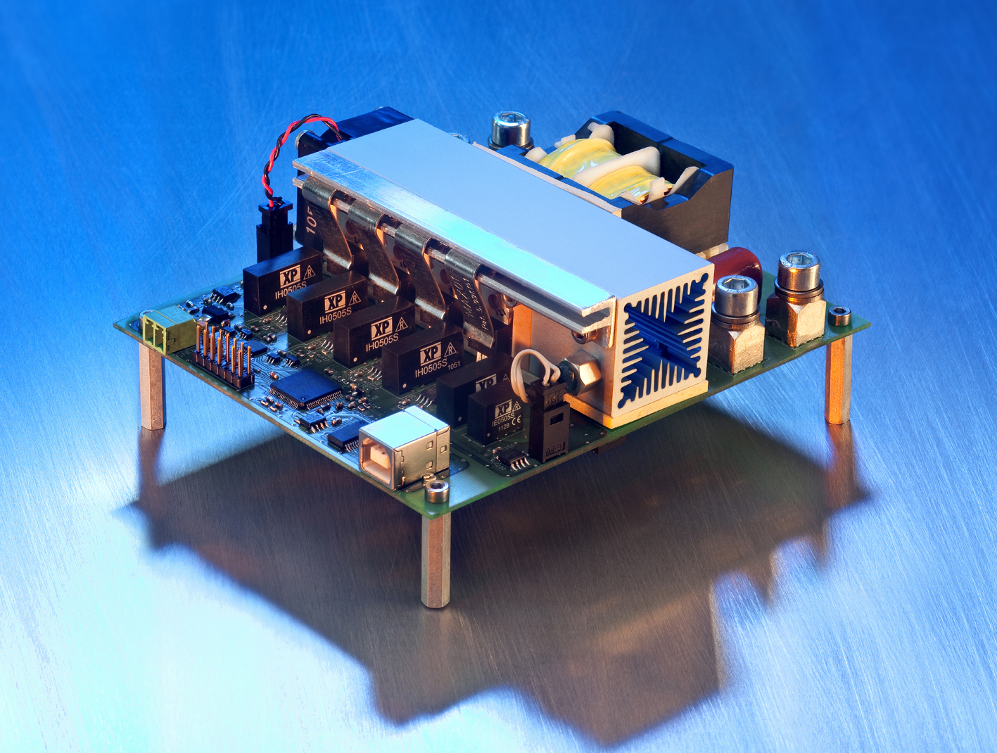
Fig. 6.4
CPES has created a design of a multichip Gallium-Nitride (GaN) power module for high-frequency power conversion (Fig. 6.5). The module is designed with the HRL 600 V Gallium-Nitride (GaN) enhancement-mode HEMT device. To exploit the capability of fast switching with low loss from high-voltage GaN devices, different layout structures have been analyzed to reduce power loop parasitic inductance and improve switching performance. The approach investigated is based on a multi-chip module where small-current-rated dies are placed in parallel to achieve higher current handling capability. Finite-element analysis (FEA) and switching circuit simulation show that the multi-layer powerloop design can effectively reduce the gate loop inductance and voltage over-shoot on the devices. This multi-layer design also improves current sharing of the multi-chip module during switching operation.(1)
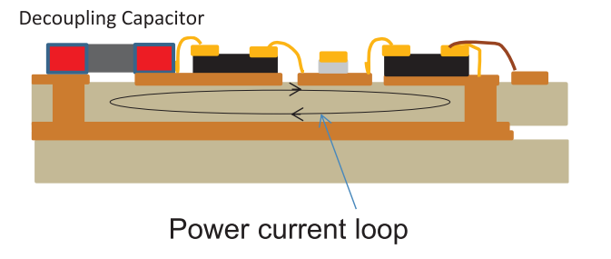
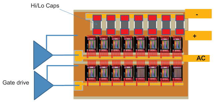
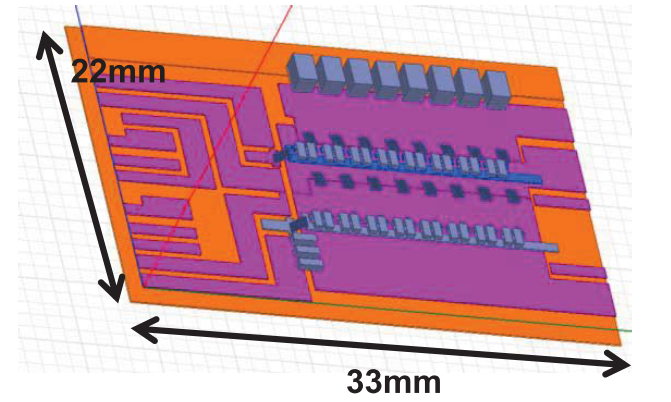
Fig. 6.5 Cascade multi-layer structure; top-left: cross section; top-right: top view; bottom-left: full picture of the module; bottom-right: final experimental converter(1)
__________________
| (1) |
Fang Luo, Zheng Chen, Lingxiao Xue, Paolo Mattavelli, Dushan Boroyevich, Brian Hughes, Design considerations for GaN HEMT multichip halfbridge module for high-frequency power converters, 2014 IEEE Applied Power Electronics Conference and Exposition - APEC 2014, [online] |
 7 Future applications
.
The past decade has witnessed tremendous progress in the development of III-nitride based light emitting diodes (LEDs) for lighting and high electron mobility transistors (HEMTs) for power applications. Sharing the same GaN-based material system, monolithic integration of HEMTs and LEDs can effectively reduce undesirable parasitics and greatly improve the system stability as well as reliability. However, there are limited reports on the monolithic integration of the two kinds of devices, probably due to the huge difference in material requirements for LEDs and transistors as well as the complexity of device fabrication. A monolithic integrated HEMT-LED device with comparable performance to stand-alone devices has been recently fabricated (Fig. 7.1) and the breakdown voltage was enhanced, without degradation of the HEMT DC performance. (1)
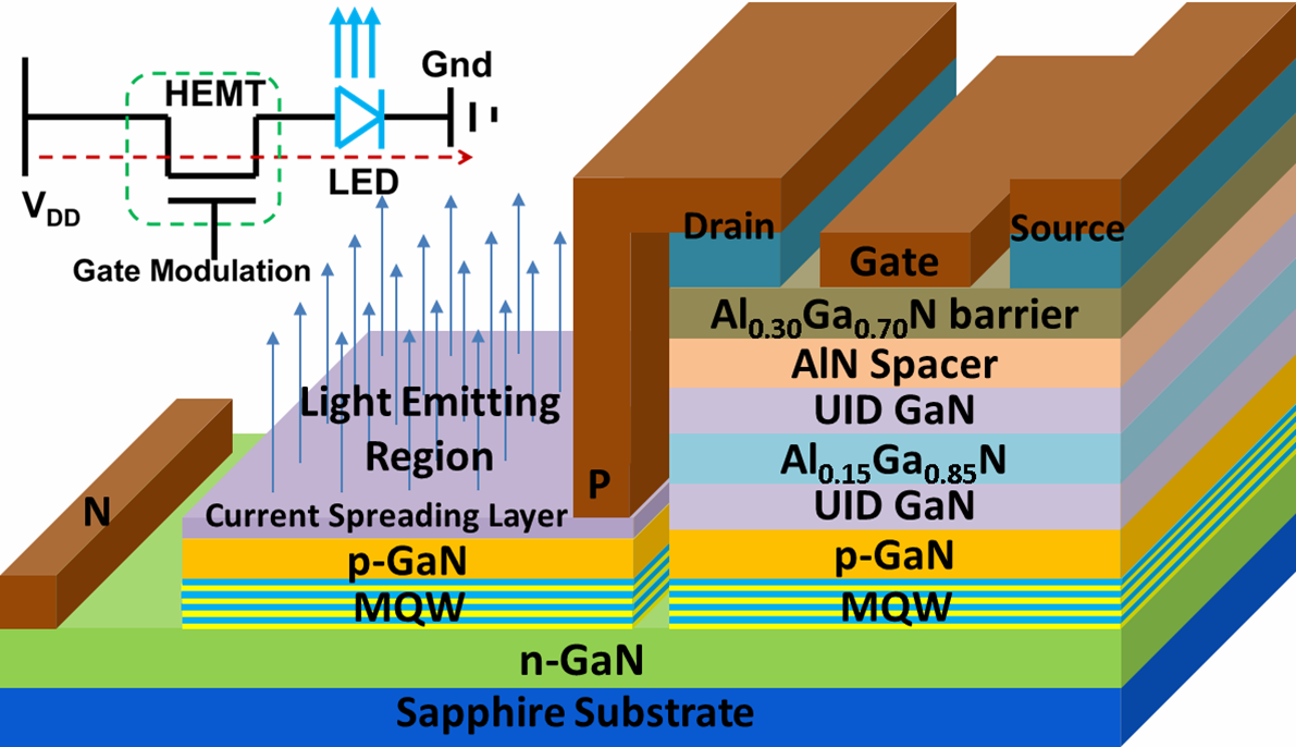
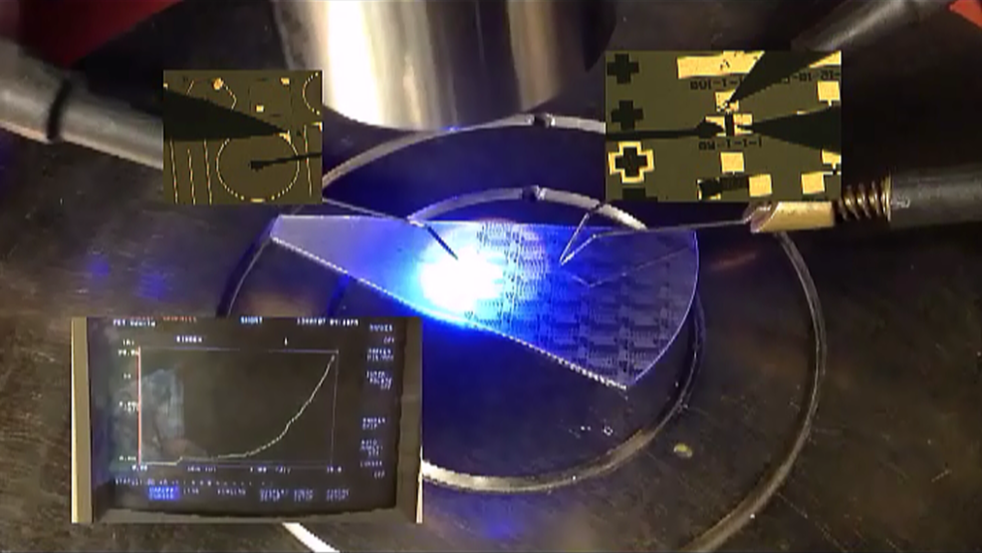
Fig. 7.1 Cross-sectional schematic of the finished HEMT-LED on sapphire substrate. The inset shows the equivalent circuit diagram of the device (left). The on-testing HEMT-LED emits blue light. The inset shows the circuit schematic of the device (right).(1)
The power electronics industry now deals with conversion and motion, and thus requires lighter/smaller, cheaper and more efficient systems. This evolution starts with improvements at the semiconductor level, and there are four technologies which are best suited to handle new system requirements: silicon IGBT, Super Junction (SJ) MOSFETs, Gallium Nitride (GaN) and Silicon Carbide (SiC)-based devices.
GaN and SiC also have a chance to outdo silicon performance and enhance inverter capabilities. However, materials are still expensive and the technology is not yet ready. On the other hand, both of these materials can benefit from their developed status in the LED industry, and we have seen plenty of LED players paying attention to the opportunity that power electronics represent.
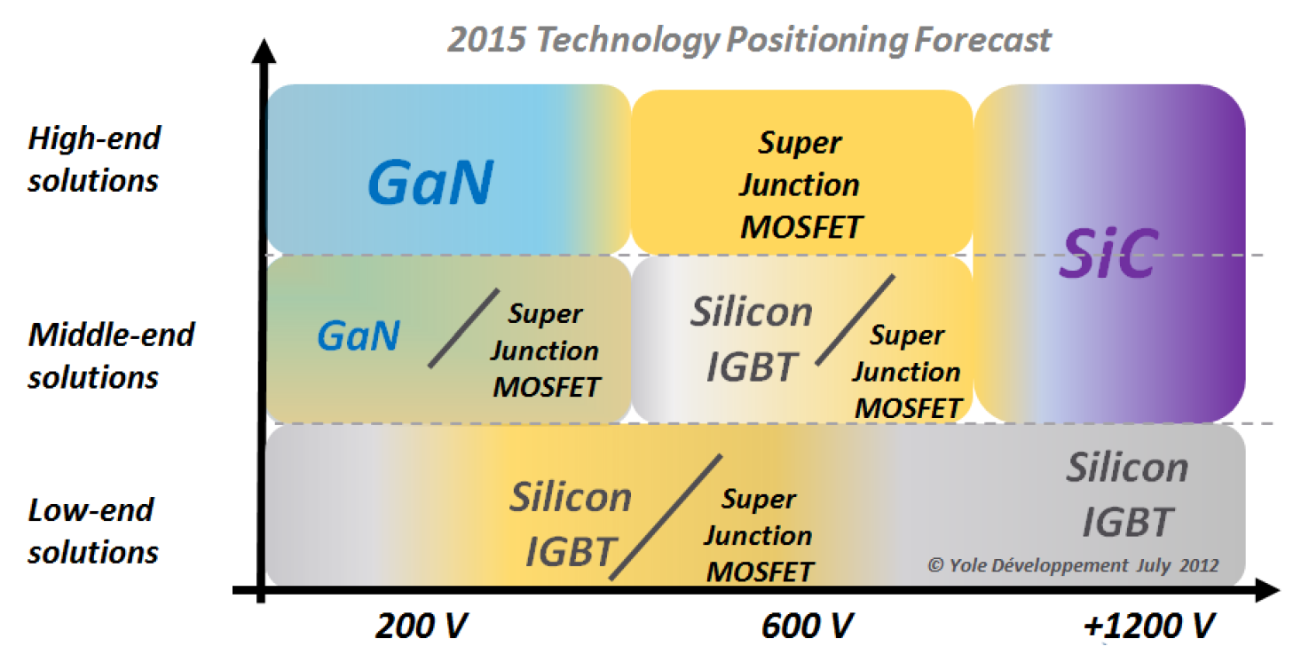
Fig. 7.2 Technology positioning depending on voltage range and system value requirements (source: Yole Développement)
__________________
| (1) |
Zhao Jun Liu,Tongde Huang, Jun Ma, Chao Liu, Kei May Lau, Monolithic Integration of AlGaN/GaN HEMT on LED by MOCVD, IEEE Electron Device Letters, Volume:35, Issue:3, January 2014, [online] |
 Reference
.
BALIGA, B.J. Advanced Power MOSFET Concepts., 2010. 562 s. ISBN 978-1-4419-5916-4.
Sanken Semiconductors, Next Generation Power Semiconductors: Sanken's Commitment to GaN/SiC Development, [online] 2013, [cit. 2015-10-10]
OSIRIS - Optimal SIC substR ates for Integrated Microwave and Power CircuitS, CORDIS. [online], 2014 [cit. 2015-10-10]
GaN to grow at 9% CAGR to over 18% of RF device market by 2020, [online]
Stephen Oliver, Optimize a Power Scheme for these Transient Times, Sep 30, 2014 [online]
Microsemi Corporation - GaN on SiC HEMT transistor 1011GN-1000V [online]
Takashi Mimura, “The Early History of the High Electron Mobility Transistor (HEMT)”, IEEE Transactions on microwave theory and techniques, Vol. 50, No. 3, March 2002.
R. Dingle et al., Appl. Phys. Lett. 33, 665 (1978).
Edward C. Niehenke, The Evolution of Transistors for Power Amplifiers: 1947 to Today, IEEE, 2015, [online]
US 4471366, Daniel Delagebeaudeuf and Trong L. Nuyen, "Field effect transistor with high cut-off frequency and process for forming same" google patents link
Takashi Mimura, Development of High Electron Mobility Transistor, Jpn. J. Appl. Phys., Vol. 44, No. 12 (2005), pp. pp. 8263–8268
M. Asif Khan et al., Appl. Phys. Lett. 60, 3027 (1992)
M. A. Khan, A. Bhattarai, J. N. Kuznia and D. T. Olson: Appl. Phys. Lett. 63 (1993) 1214
H Xing, S Keller, Y-FWu, L McCarthy, I P Smorchkova, Gallium nitride based transistors, J. Phys.: Condens. Matter 13 (2001)
S. M. Sze , Physics of Semiconductor Devices, John Wiley & Sons, Inc. (1981)
He Xiao-Guang, Zhao De-Gang, Jiang De-Sheng, Formation of two-dimensional electron gas at AlGaN/GaN heterostructure and the derivation of its sheet density expression, Chinese Physics B, 2015, 24(6): 067301 [online]
B. J. Kelley, B. C. Dodrill, J. R. Lindemuth, G. Du, J.R. Meyer, L. Faraone, Electronic Transport Characterization of HEMT Structures, Solid State Technology 43.12 (2000): 130-134. [online]
T. R. Lenka, A. K. Panda, Characteristics Study of 2DEG Transport Properties of AlGaN/GaN and AlGaAs/GaAs-based HEMT, Physics and Technology of Semiconductor 45 (5), 2011, [online]
Helmut Brech, The Principles of a HEMT, [online] 1998, [cit. 2015-10-10]
Anders Lundskog, Characterization of advanced AlGaN HEMT structures, Master thesis, 2007, [online]
M. Charfeddine, H. Belmabrouk, M. A. Zaidi, H. Maaref, 2-D Theoretical Model for Current–Voltage Characteristics in AlGaN/GaN HEMT’s, Journal of Modern Physics, Vol.3 No.8, 2012, [online]
A. Hamdoune, M. Abdelmoumene, A. Hamroun, Static and Dynamic Characteristics of an Appropriated and Recessed n-GaN/AlGaN/GaN HEMT, World Academy of Science, Engineering and Technology International Journal of Electrical, Computer, Energetic, Electronic and Communication Engineering Vol:7, No:1, 2013, [online]
Robert J. Trew, High-Frequency Solid-State Electronic Devices, IEEE TRANSACTIONS ON ELECTRON DEVICES, VOL. 52, NO. 5, MAY 2005, [online]
H. G. Henry, S-band operation of SiC power MESFET with 20 W(4.4 W/mm) output power and 60% PAE, IEEE Trans. Electron Devices, vol. 51, no. 6, pp. 839–845, Jun. 2004, [online]
R. C. Clarke and J. W. Palmour, SiC microwave power technologies, Proc. IEEE, vol. 90, no. 6, pp. 987–992, Jun. 2002, [online]
Y.-F. Wu, A. Saxler, M. Moore, R. P. Smith, S. Sheppard, P. M. Chavarkar, T. Wisleder, U. K. Mishra, and P. Parikh, 30-W/mm Gan HEMTs by field plate optimization, IEEE Electron Device Lett., vol. 25, no. 11, pp. 117–119, Nov. 2004, [online]
U. K. Mishra, P. Parikh, and Y.-F. Wu, AlGaN/GaN HEMTs-an overview of device operation and applications, Proc. IEEE, vol. 90, no. 6, pp. 1022–1031, Jun. 2002, [online]
Trew, R.J., Wide bandgap transistor amplifiers for improved performance microwave power and radar applications, 15th International Conference on Microwaves, Radar and Wireless Communications, MIKON - 2004, [online]
T. Oka, T. Nozawa, AlGaN/GaN Recessed MIS-Gate HFET With High-Threshold-Voltage Normally-Off Operation for Power Electronics Applications, IEEE ELECTRON DEVICE LETTERS, VOL. 29, NO. 7, JULY 2008, [online]
Z. H. Feng , R. Zhou, S. Y. Xie, J. Y. Yin, J. X. Fang, B. Liu, W. Zhou, Kevin J. Chen, S. J. Cai, 18-GHz 3.65-W/mm Enhancement-Mode AlGaN/GaN HFET Using Fluorine Plasma Ion Implantation, IEEE Electron Device Letters, Volume:31, Issue: 12, pp. 1386-1388, October 2010, [online]
Y. Uemoto, M. Hikita, H. Ueno, H. Matsuo, H. Ishida, M. Yanagihara, T. Ueda, T. Tanaka, D. Ueda, Gate Injection Transistor (GIT)—A Normally-Off AlGaN/GaN Power Transistor Using Conductivity Modulation, IEEE Transactions on Electron Devices, Volume:54, Issue:12, pp. 3393-3399, Dec. 2007, [online]
F. Calle, T. Palacios, E. Monroy, J. Grajal, M. Verdú, Z. Bougrioua, I. Moerman, AlGaN/GaN HEMTS: material, processing, and characterization, Journal of Materials Science: Materials in Electronics, Volume 14, Issue 5, pp 271-277, May 2003, [online]
Daniel D. Koleske, Andrew A. Allerman, S. R. Kurtz, Stephen R. Lee, Alan F. Wright, Carleton H. Seager, Nancy A. Missert, Albert G. Baca, Ronald D. Briggs, Phil F. Marsh, Chris P. Tigges, Randy J. Shul, David M. Follstaedt, and Paula P. Provencio, Materials Physics and Device Development for Improved Efficiency of GaN HEMT High Power Amplifiers., Sandia National Laboratories , December 2005, [online]
O. Deblecker, Z. De Grève and C. Versèle, Comparative Study of Optimally Designed DC-DC Converters with SiC and Si Power Devices, Advanced Silicon Carbide Devices and Processing, 2015, [online]
Douglas James Macfarlane, Design and fabrication of AlGaN/GaN HEMTs with high breakdown voltages, PhD Thesis, School of Engineering, University of Glasgow, 2014, [online]
F. Calle, T. Palacios, E. Monroy, J. Grajal, M. Verdú, Z. Bougrioua, I. Moerman, AlGaN/GaN HEMTS: material, processing, and characterization, Journal of Materials Science: Materials in Electronics, Volume 14, Issue 5, pp 271-277, May 2003, [online]
AIXTRON webpage, [online]
CHVÁLA, Aleš, DONOVAL, Daniel, ŠATKA, Alexande, MOLNÁR, Marián, MAREK, Juraj, PRÍBYTNÝ, Patrik, Advanced methodology for fast 3-D TCAD device/circuit electrothermal simulation and analysis of power HEMTs, IEEE Transactions on Electron Devices, Vol. 62, No. 3, pp. 828-834, 2015, [online]
Synopsys, San Jose, CA, USA. (1986). Technology Computer-Aided Design, [online]
CHVÁLA, Aleš, DONOVAL, Daniel, MOLNÁR, Marián, MAREK, Juraj, PRÍBYTNÝ, Patrik, Advanced methodology for fast 3-D TCAD electrothermal simulation of power HEMTs including package, SISPAD 2015 : International conference on simulation of semiconductor processes and devices, Washington DC, USA, September 9-11, Piscataway : IEEE, 2015, S. 116-119. ISBN 978-1-4673-7859-8, 2015, [online]
U. K. Mishra, P. Parikh, Yi-Feng Wu, AlGaN/GaN HEMTs-an overview of device operation and applications, Proceedings of the IEEE, Volume:90 Issue:6, 2002, [online]
saniks, HEMT, [online]
Fang Luo, Zheng Chen, Lingxiao Xue, Paolo Mattavelli, Dushan Boroyevich, Brian Hughes, Design considerations for GaN HEMT multichip halfbridge module for high-frequency power converters, 2014 IEEE Applied Power Electronics Conference and Exposition - APEC 2014, [online]
Zhao Jun Liu,Tongde Huang, Jun Ma, Chao Liu, Kei May Lau, Monolithic Integration of AlGaN/GaN HEMT on LED by MOCVD, IEEE Electron Device Letters, Volume:35, Issue:3, January 2014, [online]