 5 HEMT design and fabrication
5.3 Transistor fabrication layout
.
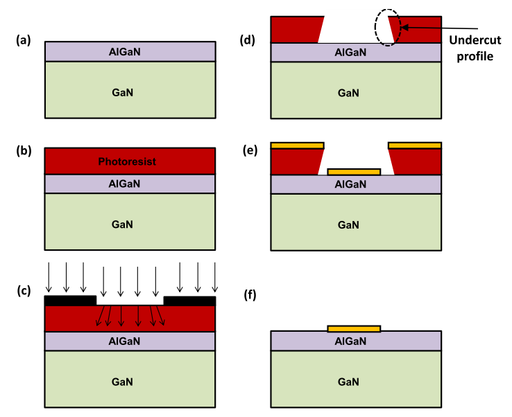
The following sections will outline the processes required to take an epitaxially grown wafer through to the completed working device stage. Fig. 5.4 shows the process flow for photolithography and metallisation and should be referred to when reading the following sections.

Fig. 5.4 Device process (a) Sample has been cleaned and is ready to be processed (b) Photoresist is spun onto sample (c) Sample has been soaked in developer solution and is now being subjected to UV light. The black boxes on top of the photoresist indicate the mask plate in contact with the sample, protecting areas which do no require to be patterned (d) Photoresist is developed and shows an undercut profile which will benefit the metal lift-off process (e) The sample is then metallised in the electron beam evaporator (f) Finally the sample is immersed in warm acetone to remove the photoresist and leave behind only the metal which was evaporated directly onto the material.
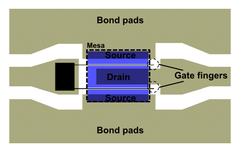
The layout of a typical RF transistor unit cell for research purposes consists of two gate fingers and is shown in Fig. 5.5 (when implemented for amplifiers etc. the number of fingers will increase to increase the output current/power). When fabricating many RF devices on the same sample of material, a mesa isolation step is required to electrically isolate them from one another on the sample.(1)

Fig. 5.5 Typical layout of unit cell of RF device which has two gate fingers.
__________________
| (1) | Douglas James Macfarlane, Design and fabrication of AlGaN/GaN HEMTs with high breakdown voltages, PhD Thesis, School of Engineering, University of Glasgow, 2014, [online] |