 3 HEMT basic
3.2 Properties of the 2DEG
.
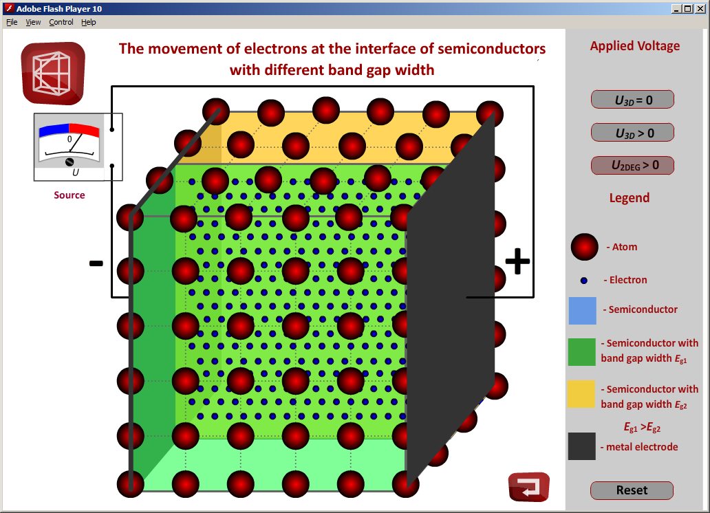
HEMTs unlike MOSFETs incorporates a so called 2DEG as the conducting channel. This 2DEG is formed at the heterojunction of the semiconductor structure and is always present as described in previous chapter. The key factor of the 2Deg or two dimensional electron gas is in its spatial confinement in the third dimension constraining electrons to move freely only in two dimension consisting only of conducting electrons which are distant from their parent atoms because of polarization effects in the structure.(1) Electrons can thus travel several micrometers before colliding into lattice of the semiconductor where the 2DEG is formed (Fig. 3.5). This collision-free environment in combination with low effective mass of electrons gives an extremely high mobility system (sometimes called “hot” electrons), which can be applied in fast electronic devices. Especially at low temperatures the mobility can be in orders of 1 000 000 cm2/Vs. This makes possible for 2Deg to have superior material properties such as high break-down electric field (5 MV/cm), high thermal conductivity (1.3 Wcm-1C-1), high peak velocity (>3x107cm-1s), high saturation velocity (>1.5x107cm-1s), and high sheet charge density (1x1013cm-2).(2)
Fig. 3.5 Electron movement in bulk and hetero structure (click to run)
__________________
| (1) | B. J. Kelley, B. C. Dodrill, J. R. Lindemuth, G. Du, J.R. Meyer, L. Faraone, Electronic Transport Characterization of HEMT Structures, Solid State Technology 43.12 (2000): 130-134. [online] |
| (2) | T. R. Lenka, A. K. Panda, Characteristics Study of 2DEG Transport Properties of AlGaN/GaN and AlGaAs/GaAs-based HEMT, Physics and Technology of Semiconductor 45 (5), 2011, [online] |
