Hi Guest user!
 |
6.2System in package |
The assembly of the RF transceiver, especially for the TX part (which includes the Power Amplifier) depends on the frequency range and application. Of course, the frequency as well as the power density level are very important criteria, which will define the technology choice for each chip and the overall Packaging architecture. One recent trend observed for many markets is a demand for small size heterogeneous integration (SiP) at low cost. This can be obtained by using organic materials for both the PCB substrate and for the package substrate, as shown in Fig. 6.4.
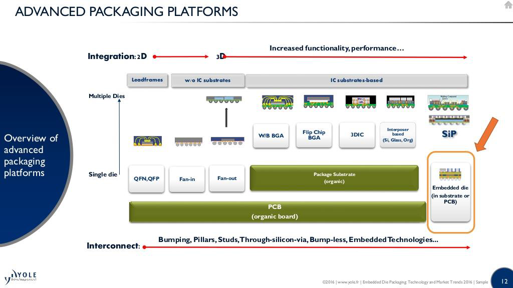
Fig. 6.4: Advanced packaging platforms (source: Yole report, 2016).
System in Package based on organic interposer platform using 3D technologies interconnection is considered as a valid approach for achieving 5G transceiver. It consists in the heterogeneous integration of Silicon CMOS driver chips, GaN Power Amplifier and passive elements in a same package.
The main advantages for this approach are listed below:
- Highly integrated architecture and reduced footprint of the module
- Optimized low loss RF links between the active chips with short interconnects and built-in matching and decoupling network
- Possibility to integrate active and passive elements for decoupling and matching network; at a first stage passive RLC elements and antenna should be considered but active filters and switchers can be also implemented in the interposer in the future
- Wafer level solutions for interconnect and packaging would give competitive advantages in term of aggressive process capability and overall cost in HVM.
In the scope of this project we propose to consider different approaches of packaging for building this SIP module based on organic materials:
- An organic laminate LGA type substrate with chip embedded technology
- A fan-out wafer level packaging using molding compound, also having embedded chip principle.
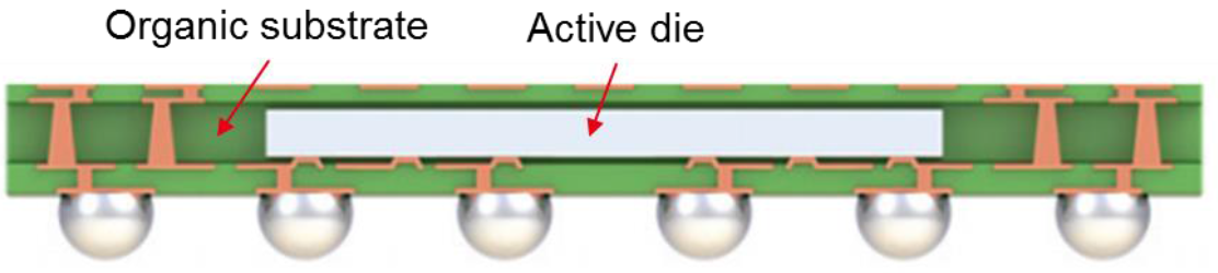
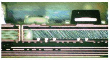
The first approach will be using embedded die technology in organic laminate substrate commonly named “LGA” for Land grid array referring to the termination of the substrate as link to the application board. This technology is already largely adopted in many field of consumer applications as illustrated in these pictures on Fig. 6.5.
 |
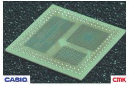 |
Fig. 6.5: Illustration of embedded die technology in organic laminate substrate.
But, the RF applications considered in this project are still at a development stage. Early development studies can be found in the literature as the work carried out recently at Georgia institute of technology [1] for example. Note that in this work only the GaN Power amplifier is integrated in the organic substrate, our ambition is to integrate a multi-chip module and active and passive elements.
Moreover the aim will be to introduce new added value features to this package to address the specific challenges of mm-wave and high power devices such as RF transmission efficiency and thermal management for example.
The second approach will be using a Fan-out wafer level packaging (FOWLP) technology based on epoxy molding compound material.
Standard eWLB process flow is based on a chip first approach which flow is illustrated hereafter figure 13. It is composed of 2 main blocks:
- Molding strata fabrication with embedded dies
- Fan-out RDL fabrication on top of the strata with can have 1 to plural levels of metal.
On top of last level of metallization UBM is formed for solder ball placement. Cu/solder bumps can be alternatively substituted to solder balls if needed.
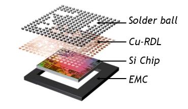
Fig. 6.7: eWLB exploded view (from STAT Chip Pac)
Today another approach has been introduced in the market which is based on RDL first flow described below Fig. 6.8.
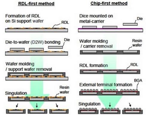
Fig. 6.8: RDL first vs Chipfirst technologies
This last approach allows thinner pitch RDL since the process is done on a rigid carrier substrate on not on the molding material and also offer the advantage of assessing the interposer yield before stacking avoiding to lose good active dies and last it has thinner package capability.
More activities are today pursued on RDL first approach using the fabrication line capability installed in MINATEC including RDL build up, through mold via (TMV) and molding film lamination.
_____________________________________________________________
[1] K. Takinami, "A 60GHz wireless transceiver employing hybrid analog/digital beamforming with interference suppression for multiuser Gigabit/s radio access", 2015 Symposium on VLSI Circuits (VLSI Circuits), June 2015.
Table of contents
Navigation
Site pages
Courses
Settings
Book administration