Hi Guest user!
 3 HEMT basic
3.5 Types of HEMTs
.
III-V compound semiconductors are mainly used in HEMT’s as heterojunction materials for channel formation as shown in Fig. 3.7. The name high electron mobility transistor is derived from its high electron mobility nature which is a result of a quantum well (a special kind of potential well) near the hetero interface. In this well the conduction channel is a two dimensional electron gas (2DEG) instead of a three dimensional structure like in conventional FETs. As a result, it has significantly less Coulomb scattering, resulting in a very high mobility device structure.
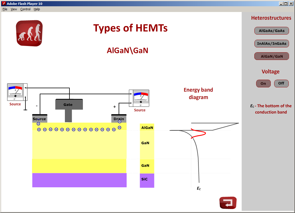
Fig. 3.7 Types of commonly used HEMTs (click to run)
Ideally, the two different materials used for a heterojunction would have the same lattice constant (spacing between the atoms). In practice, e.g. AlGaAs on GaAs, the lattice constants are typically slightly different, resulting in crystal defects. As an analogy, imagine pushing together two plastic combs with a slightly different spacing. At regular intervals, you'll see two teeth clump together. In semiconductors, these discontinuities form deep-level traps, and greatly reduce device performance.
A HEMT where this rule is violated is called a pseudomorphic HEMT or pHEMT. This is achieved by using an extremely thin layer of one of the materials – so thin that the crystal lattice simply stretches to fit the other material. This technique allows the construction of transistors with larger bandgap differences than otherwise possible, giving them better performance.
Another way to use materials of different lattice constants is to place a buffer layer between them. This is done in the metamorphic HEMT or mHEMT, an advancement of the pHEMT. The buffer layer is made of AlInAs, with the indium concentration graded so that it can match the lattice constant of both the GaAs substrate and the GaInAs channel. This brings the advantage that practically any Indium concentration in the channel can be realized, so the devices can be optimized for different applications (low indium concentration provides low noise; high indium concentration gives high gain).
In contrast to a modulation-doped HEMT, an induced HEMT provides the flexibility to tune different electron densities with a top gate, since the charge carriers are "induced" to the 2DEG plane rather than created by dopants. The absence of a doped layer enhances the electron mobility significantly when compared to their modulation-doped counterparts. This level of cleanliness provides opportunities to perform research into the field of Quantum Billiard for quantum chaos studies, or applications in ultra stable and ultra sensitive electronic devices.
Table of contents
Navigation
Site pages
Courses
Archív Elektronika
Settings
Book administration
Course administration