 5 HEMT design and fabrication
5.4 Growth challenges
.
Several growth techniques are used to fabricate AlGaN/GaN HEMTs. Among all the most used are metal organic vapor phaze epitaxy (MOCVD) which provides best material properties and molecular beam epitaxy (MBE) with the advantage of improved interface quality. Whatever the substrate or the technique is being used, material growth is a key challenge for the device operation. (1)
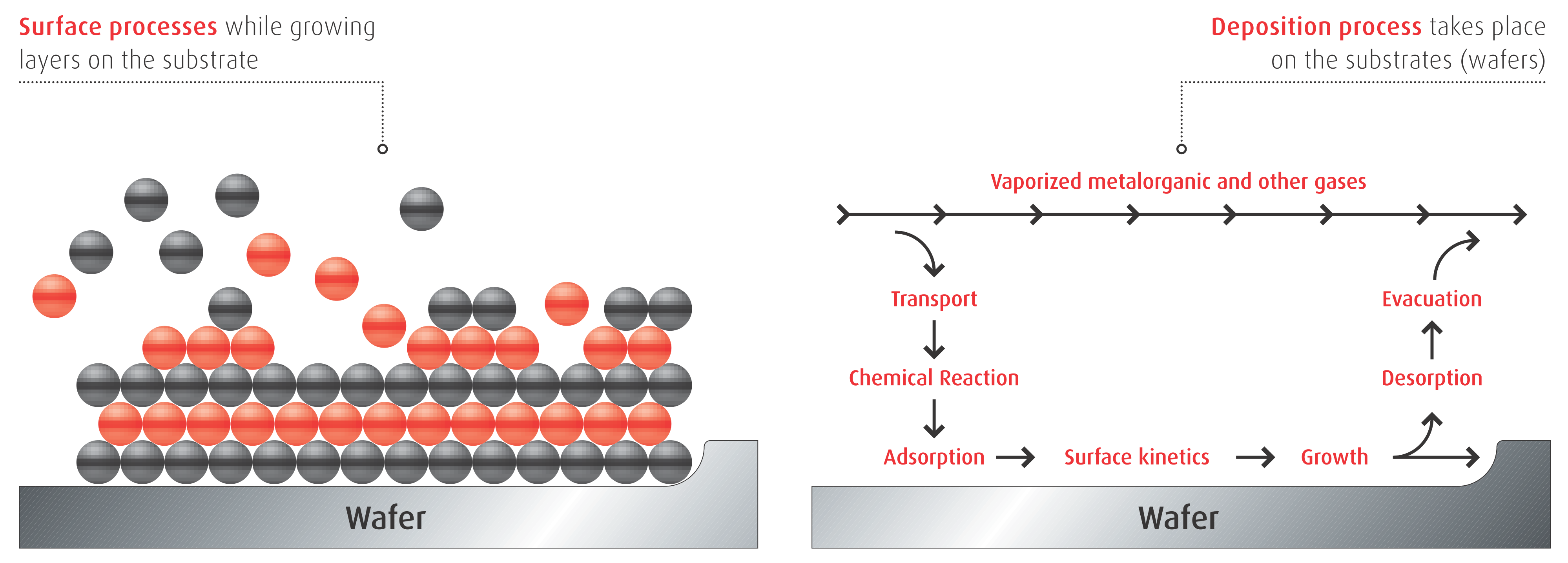
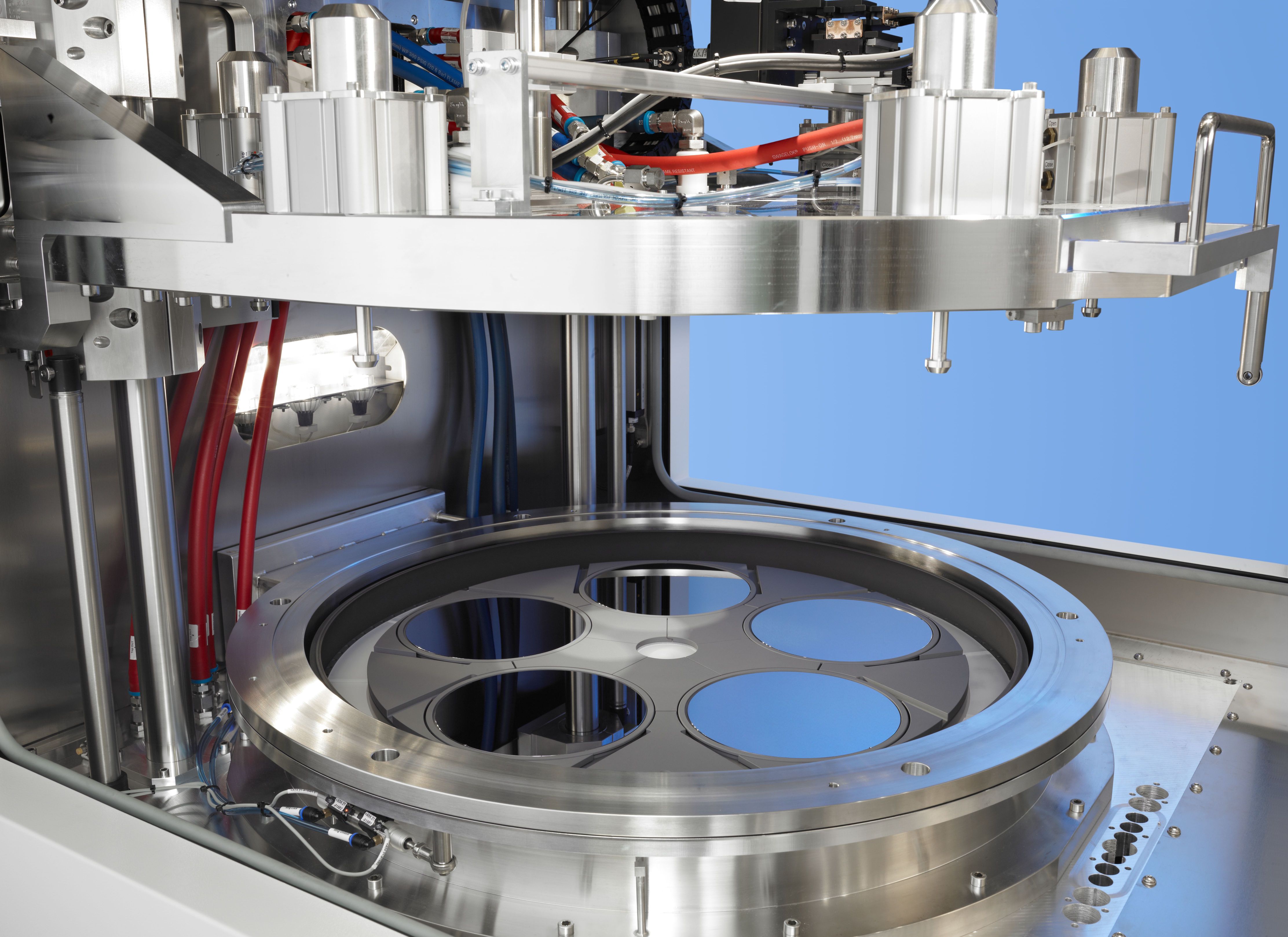
Fig. 5.6 MOCVD epitaxy principle and AIX G5+ reactor chamber(2)
MOCVD has been the most commonly used technique for developing GaN based epilayers and is carried out at temperatures in excess of 1000◦C and involves gaseous reactants (such as trimethylgallium and NH3) passing over a heated substrate which react to form a condensed layer or film on the substrate. Growth rates are typically between 1 - 2 µm per hour. MBE on the other hand, is a slower process with growth rates typically between 0.5 - 1 µm per hour and is carried out at lower temperatures compared to MOCVD (500 - 900◦C). MBE uses solid Ga and Al sources along with NH3 and occurs via reactions between thermal-energy molecular, atomic, or ionised beams of the constituent elements on a heated substrate in an ultra-high vacuum.(3)
The major technical issues associated with GaN HEMT technology are the presence of defects including traps and dislocations, thermal management of the operating devices, dislocations near the active regions, and growth and device fabrication reproducibility.
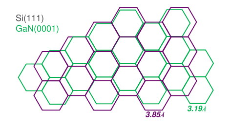
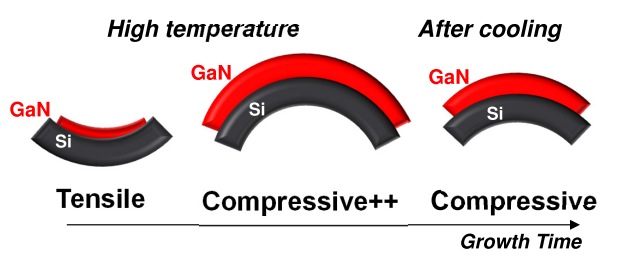
Fig. 5.7 Difficulties of growing GaN on Si because of lattice mismatch (left) and thermal expansion mismatch (right)(5)
Defects are introduced into the HEMT structure during the growth. The most common defects that occur in GaN are dislocations, impurities, and point defects. Dislocations originate in GaN at the hetero-interface partly due to the lattice mismatch between SiC and GaN and partly due to the discrete GaN grains, which form and ultimately coalesce on the SiC to form the film. Dislocations in GaN typically range from 10 8 to 10 10 cm -2 and this density is independent of growth technique. Impurities and point defects on the other hand are more strongly influenced by the reactor growth conditions. Each of these defects can adversely affect device performance by creating charge trapping centers and leakage pathways, which can ultimately lead to device failure and reliability issues.
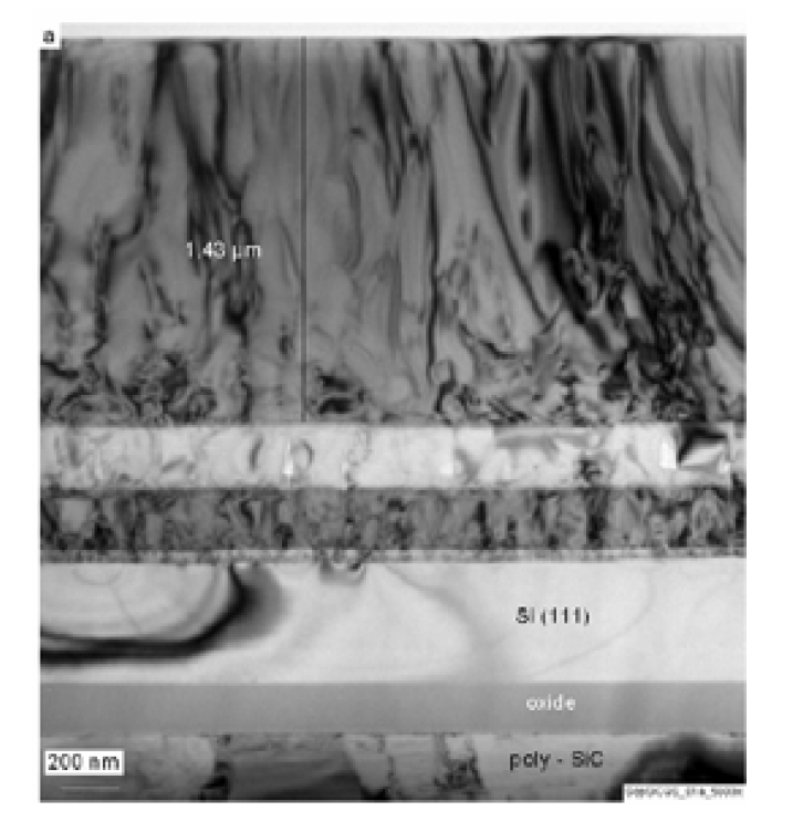
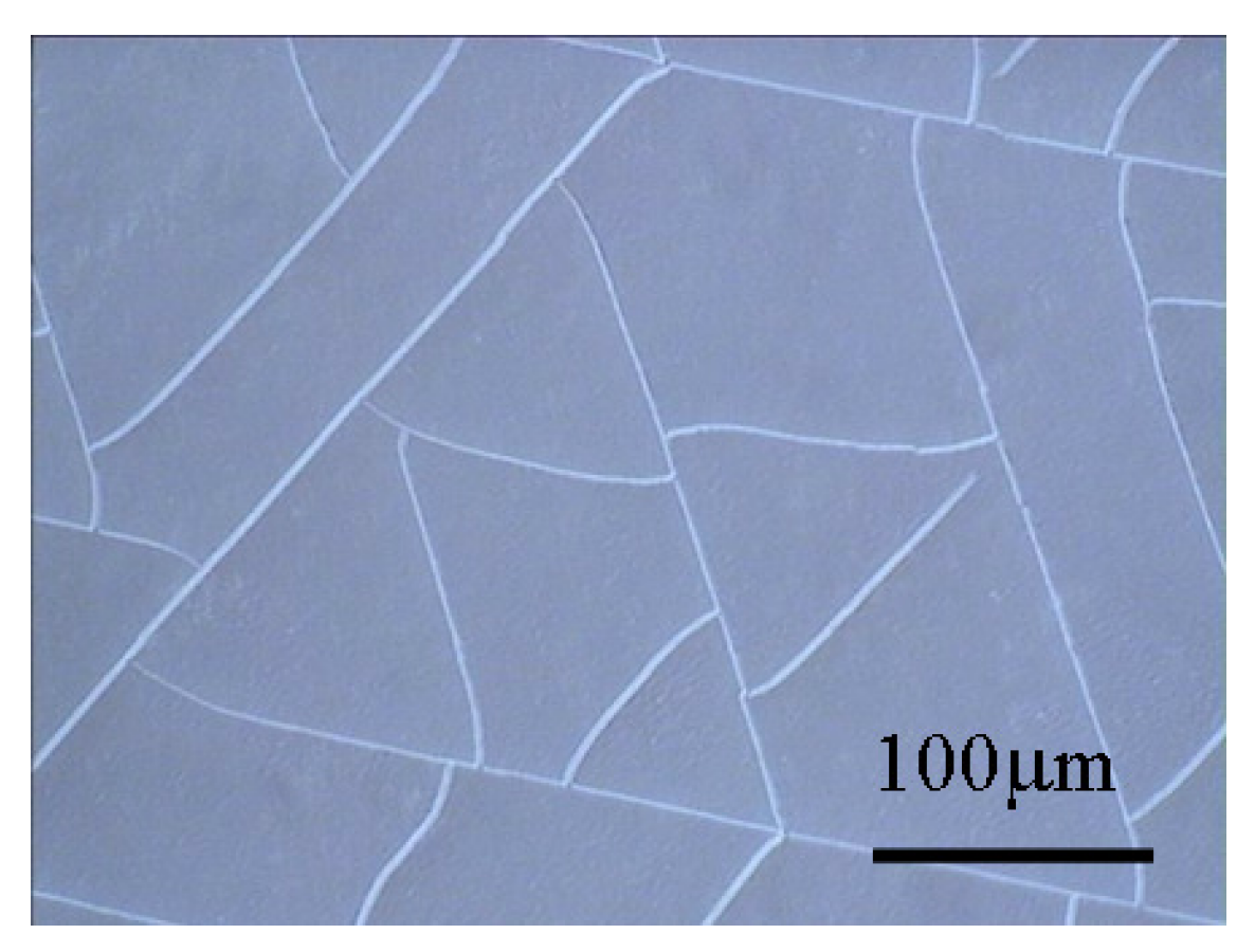
Fig. 5.8 Consequences of lattice mismatch leading to defects in the structure (left)(6) and thermal expansion mismatch leading to GaN layer cracking on a surface (right)(5)
Trapping type defects can dramatically limit frequency performance, especially in the GaN or AlGaN layers near the two dimensional electron gas (2-DEG). For a HEMT to work properly the GaN must be insulating enough such that current flows only through the 2-DEG and not in parallel through the bulk GaN. If on the other hand, the semi-insulating (SI) GaN is too resistive electron traps may be present in the GaN. Traps can also produce current collapse in HEMT devices, which is caused when hot electrons are injected into the insulating GaN region. Once trapped, the electrons cannot be thermally emitted because of the large bandgap. As a result the electrons effectively back gate the device, leading to reduced current flow in the 2-DEG. In addition to hot electron injection, cycling either the gate or drain voltage can cause transient reductions in the drain current. Traps are also likely present in the AlGaN and at surface of HEMTs. Traps may result from impurity, vacancy, or dislocation structures. Ultimately, these traps limit gain, linearity, power-added-efficiency, reproducibility, and reliability in GaN-based HEMT devices. To date, not been much progress has been made in solving these trap related issues that influence rf-dispersion.
Ideally, bulk GaN substrates could reduce or eliminate the influence of trapping type defects on HEMT performance, especially traps associated with dislocations. However, during operation junction temperatures of HEMTs are greater than 200 ºC, which can lead to device breakdown and loss of linearity. This suggests that active cooling of the devices is potentially as important as reducing the influence of traps. Because SiC has a high thermal conductivity and is closely lattice matched GaN (3.5% difference) and AlN (< 1% difference), SiC is the best substrate for GaN HEMTs. To date the GaN HEMTs with the best power performance have been grown on SiC.
The main issue with GaN heteroepitaxy on SiC is that threading dislocations are formed in the GaN. 100 nm of AlN is first grown on the SiC to provide nucleation sites and enhance two dimensional growth of the GaN. Growth of the AlN layer generates primarily edge type dislocations resulting from the discrete granularity of the AlN film. These edge dislocations can then propagate through the GaN and AlGaN films. While these dislocations are benign to transport in the 2-DEG they can limit the maximum source-drain voltage and provide shorting pathways within the device. Additional misfit dislocations can be generated at the AlGaN/GaN interface, especially when the Al concentration exceeds 30%. Techniques to reduce dislocations, such as epitaxial lateral overgrowth (ELOG), have not been extensively studied for improving HEMT performance.
Finally, there are many issues associated with the growth and characterization GaN HEMTs on SiC that have not yet been identified or addressed. In general, the growth and theory of how semi-insulating (SI) GaN is produced on SiC is not well controlled or understood. Surprisingly, some researches in the field have suggested that the GaN grain structure may play a pivotal role in achieving SI GaN. If this is the case, then reproducible nucleation of the GaN to replicate the same grain structure is absolutely necessary. Understanding of the physics behind the operation of GaN HEMTs is also lacking. This is primarily because physics measurements of the HEMT material properties are difficult and models of HEMTs with traps, dislocations, and surface charge have not been developed. (4)
__________________
| (1) | F. Calle, T. Palacios, E. Monroy, J. Grajal, M. Verdú, Z. Bougrioua, I. Moerman, AlGaN/GaN HEMTS: material, processing, and characterization, Journal of Materials Science: Materials in Electronics, Volume 14, Issue 5, pp 271-277, May 2003, [online] |
| (2) | AIXTRON webpage, [online] |
| (3) | Douglas James Macfarlane, Design and fabrication of AlGaN/GaN HEMTs with high breakdown voltages, PhD Thesis, School of Engineering, University of Glasgow, 2014, [online] |
| (4) | Daniel D. Koleske, Andrew A. Allerman, S. R. Kurtz, Stephen R. Lee, Alan F. Wright, Carleton H. Seager, Nancy A. Missert, Albert G. Baca, Ronald D. Briggs, Phil F. Marsh, Chris P. Tigges, Randy J. Shul, David M. Follstaedt, and Paula P. Provencio, Materials Physics and Device Development for Improved Efficiency of GaN HEMT High Power Amplifiers., Sandia National Laboratories , December 2005, [online] |
| (5) | Y. Saripalli, IEEE-ICEE 2014 |
| (6) | T. J. Anderson, F. Ren, L. Voss, M. Hlad, B. P. Gila, S. J. Pearton, J.Kim, J. Lin, P. Bove, H. Lahreche, J. Thuret and R. Langer, AlGaN/GaN High Electron Mobility Transistors and Diodes Fabricated on Large Area Silicon on poly-SiC (SopSiC) Substrates for Lower Cost and Higher Yield , CS MANTECH Conference, May 14-17, 2007, [online] |