Hi Guest user!
 5 HEMT design and fabrication
5.6 3D simulations
.
Multifinger HEMT devices with compact layout are required for high-power operation, however, self-heating induced thermal crosstalk between individual gate fingers becomes serious, which degrades device performance or results in irreversible damage. Therefore, thermal management is crucially important to the viability of power HEMTs.
Our proposed methodology for fast 3-D device electrothermal simulation is based on direct coupling between finite element method (FEM) thermal and circuit electrical simulation using mixed-mode setup(1) supported in Synopsys TCAD Sentaurus environment(2). The mixed-mode setup allows direct interconnection of a 3-D FEM thermal model of the whole system (semiconductor layers, package, printed circuit board (PCB) up to cooling assemblies), 3-D FEM electrical model of the metallization layers and an equivalent electrical temperature dependent circuit model of the HEMT (Fig. 5.9)(3).
This approach combines the speed and accuracy, and couples temperature and current density nonuniformity in structure and metallization layers. The 3-D FEM model of the structure based on the physical and geometrical description of all semiconductor and metallization layers corresponding to the real device is created in Synopsys device editor. The metallization layers are created by Synopsys layout editor, which allows viewing and editing the layouts in most of the industry-standard formats including GDSII.
The advantages of the proposed method are the relative simplicity of implementation, the speed of simulation and the capability of a full analysis of complex structures. The effects of structure design and fabrication parameters including semiconductor layers, metallization, package, and up to cooling assemblies are studied.
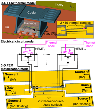
Fig. 5.9 Circuit diagram of the electrothermal mixed-mode simulation. Equivalent HEMT circuit model is connected to 3-D thermal model by the thermal nodes. Heat flux and temperature exchange is provided via thermal nodes. The current density distribution and the voltage drop on parasitic resistances are solved in 3-D electrical model of the metallization.
Fig. 5.10 a shows a comparison of the measured and simulated output characteristics for two different measurement setups. The first setup connects only Source 1 to the ground and only one gate finger is active. The second setup connects both sources to the ground and both gate fingers are active. The temperature interaction between the gate fingers for the second setup shows a drop of the output characteristics, which is caused by a higher structure temperature compared to the first setup (Fig. 5.10 c (Cross section A)). Moreover, there is an additional voltage drop due to the metal resistance caused by doubled current flowing through drain metallization layer (Fig. 5.10 b). Its main impact is in the linear region of the output characteristics. The proposed 3-D electrothermal simulation splits the structure along the gate into several parts, which allows analysis of the inhomogeneous distribution of temperature and of the electrical properties. The inhomogeneous distributions of temperature and current along the gate electrode are shown in Fig. 5.10 c (Cross section B). The lower temperature and higher current density at the HEMT edge segments are caused by more effective cooling of the structure edges compared with the central segment.
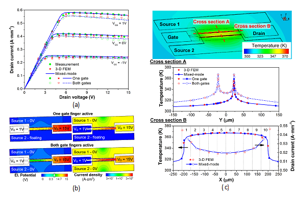
Fig. 5.10: (a) Comparison of measured and simulated output characteristics and (b) electrostatic potential and current density distribution in the metallization for one and both gate fingers active. For both gate fingers active is an additional voltage drop due to the metal resistance caused by doubled current flowing through drain metallization layer. (c) Temperature distribution of the HEMT for VDS = 15 V and VGS = 1 V (top). (Cross section A) Comparison of the temperatures across the gate electrodes for one and both gate fingers active. (Cross section B) Temperature and current distributions inside the HEMT structure along the gate electrode.
__________________
| (1) | CHVÁLA, Aleš, DONOVAL, Daniel, ŠATKA, Alexande, MOLNÁR, Marián, MAREK, Juraj, PRÍBYTNÝ, Patrik, Advanced methodology for fast 3-D TCAD device/circuit electrothermal simulation and analysis of power HEMTs, IEEE Transactions on Electron Devices, Vol. 62, No. 3, pp. 828-834, 2015, [online] |
| (2) | Synopsys, San Jose, CA, USA. (1986). Technology Computer-Aided Design, [online] |
| (3) | CHVÁLA, Aleš, DONOVAL, Daniel, MOLNÁR, Marián, MAREK, Juraj, PRÍBYTNÝ, Patrik, Advanced methodology for fast 3-D TCAD electrothermal simulation of power HEMTs including package, SISPAD 2015 : International conference on simulation of semiconductor processes and devices, Washington DC, USA, September 9-11, Piscataway : IEEE, 2015, S. 116-119. ISBN 978-1-4673-7859-8, 2015, [online] |
Table of contents
Navigation
Site pages
Courses
Archív Elektronika
Settings
Book administration
Course administration