Hi Guest user!
 1 Motivation
1.1 Project Osiris
OSIRIS project (Optimal SIC substRates for Integrated Microwave and Power CircuitS)(1), a Research and Innovation Action (RIA), aims at improving substantially the cost effectiveness and performance of gallium nitride (GaN) based millimetre wave components.
OSIRIS project will demonstrate significantly more reliable and higher efficiency devices through an innovative solution by producing GaN High Electron Mobility Transistors (HEMTs) and SiC devices using isotope-enriched, semi-insulating (SI) silicon carbide (SiC) substrates, that manifest higher thermal conductivity and lower costs specifically for GaN microwave applications. The novelty of OSIRIS project is to utilize an ingenious way of increasing the thermal conductivity of the substrate and hence the power efficiency of the HEMT device by removing all but one of the isotopes for Si and C, respectively. The thermal conductivity of the SiC substrate will make a significant leap by about 30% which plays an important role for all devices.
OSIRIS project will allow reinforcing GaN technology penetration into the market by cost effectiveness of the SiC substrates and circuit performances improvement thanks to better heat spreading close to the dissipative area. For microwave GaN/SiC HEMT this isotopic approach could create a complete shift in the currently used substrate / GaN epi-wafer technology; it intends to grow high thermal conductivity (+30%) semi-insulating SiC on top of low cost semiconducting SiC substrates (widely used by the power electronics and LED industries). Reduced layer thickness is necessary as only the top 50 to 100 µm SiC wafer is really useful as the substrate itself is currently thinned to realise microstrip waveguided microwave circuits (Fig.1.3).
For power electronics, this isotopic innovation will be essentially focused on thermal improvement, i.e. better electron mobility at a given power dissipation as mobility and drift mobility decrease with temperature and also better carrier transport thanks to lower scattering rates. Schottky and p-i-n diodes will be tested using this material, which however will have to be doped while microwave devices need semi-insulating materials.
One of the important goals of OSIRIS project is to disseminate discoveries and achievements of current high level research through various ways. Within the mission it is very important to teach young scholars at Middle schools and Universities about state of the art novelties and advanced research inventions.
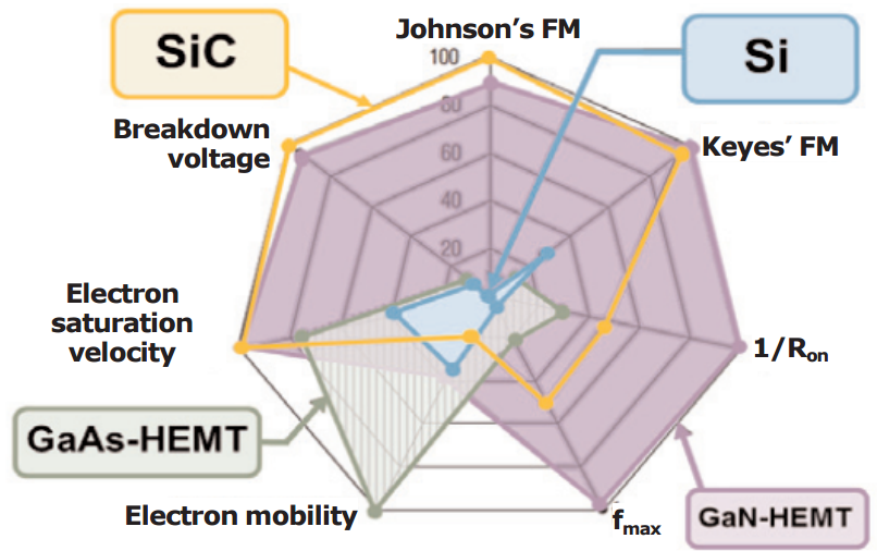
Fig. 1.3 Comparison of GaN/SiC/Si/GaAs high-power RF transistors, OKI Semiconductors, May 2014(2)
__________________
| (1) | OSIRIS - Optimal SIC substR ates for Integrated Microwave and Power CircuitS, CORDIS. [online], 2014 [cit. 2015-10-10] |
| (2) | GaN to grow at 9% CAGR to over 18% of RF device market by 2020, [online] |
Table of contents
Navigation
Site pages
Courses
Archív Elektronika
Settings
Book administration
Course administration