Hi Guest user!
 2 HEMTs invention
2.1 History
.
- In the 1979 Takashi Mimura and colleagues developed the first HEMT (AlGaAs/GaAs system) at Fujitsu in Japan. The HEMT was based on the concept of modulation doping first demonstrated by Ray Dingle and his collaborators at Bell Labs in 1978.(1,2)
- In Europe, Daniel Delagebeaudeuf and Trong Linh Nuyen from Thomson-CSF (France) filed for a patent of this device on the 28th of March 1979.(3)
- In 1980 Takashi Minura, Fujitsu laboratories designed the features of the first HEMT.
- In 1981 Fujitsu had demonstrated the first HEMT integrated circuit featuring an enhancement/depletion-mode logic ring oscillator that showed a switching delay of 17.1 ps, “the lowest of all the semiconductor logic technologies reported thus far” (Fig. 2.2).
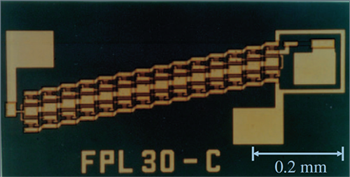
Fig. 2.2 First HEMT integrated circuit: 27-stage ring oscillator
- In 1985 the manufacturing capabilities had grown to such a level that the HEMT structure was announced as the device with the lowest noise characteristics in the world.
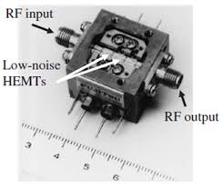
Fig. 2.2 First commercial HEMT: cryogenic low-noise amplifier for radiotelescope at Nobeyama Radio Observatory(4)
- In 1987 - Commercialization of HEMTs significantly increased in Japan and Europe and HEMTs began to replace GaAs MESFETs in broadcasting satellite receivers. HEMTs made it possible to reduce the size of a parabolic antenna by one-half or more.
- In 1988 - HEMT multibit data registers(5) were developed for the supercomputer of the National Research and Development Program of Japan.
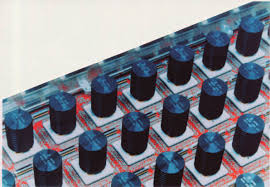 Fig. 2.3. HEMT multibit data registers mounted on circuit board of supercomputer.
- Early Applications: Low noise amplifiers (Installed in radio telescope), other space and military applications, satellite broadcasting receivers. The transistor quickly gained popularity and spread all over the world.
- In 1993 Asif Kahn demonstrated the first AlGaN/GaN HEMT.(6)
- Commercial production took off in the 90’s. In the last 30 years, HEMTs have been demonstrated in several material systems, most notably AlGaAs/GaAs and AlGaN/GaN.(7)
__________________
| (1) | R. Dingle et al., Appl. Phys. Lett. 33, 665 (1978). |
| (2) | Edward C. Niehenke, The Evolution of Transistors for Power Amplifiers: 1947 to Today, IEEE, 2015, [online] |
| (3) | US 4471366, Daniel Delagebeaudeuf and Trong L. Nuyen, "Field effect transistor with high cut-off frequency and process for forming same" google patents link |
| (4) | Takashi Mimura, Development of High Electron Mobility Transistor, Jpn. J. Appl. Phys., Vol. 44, No. 12 (2005), pp. pp. 8263–8268 |
| (5) | M. Asif Khan et al., Appl. Phys. Lett. 60, 3027 (1992) |
| (6) | M. A. Khan, A. Bhattarai, J. N. Kuznia and D. T. Olson: Appl. Phys. Lett. 63 (1993) 1214 |
| (7) | H Xing, S Keller, Y-FWu, L McCarthy, I P Smorchkova, Gallium nitride based transistors, J. Phys.: Condens. Matter 13 (2001) |
Skip Table of contentsSkip NavigationSkip Settings
Table of contents
Navigation
Site pages
Courses
Archív Elektronika
Settings
Book administration
Course administration