Hi Guest user!
 3 HEMT basic
3.1. Formation of the 2DEG
.
Basic HEMT structure widely used to explain the formation of 2Deg (two dimensionasl electron gas) consist of a GaN/AlGaN heterojunction. Heterojunction is a special type of junction between two different semiconductors, i.e. it is a junction formed by two semiconductors with different band gaps shown on Fig. 3.2.(1)
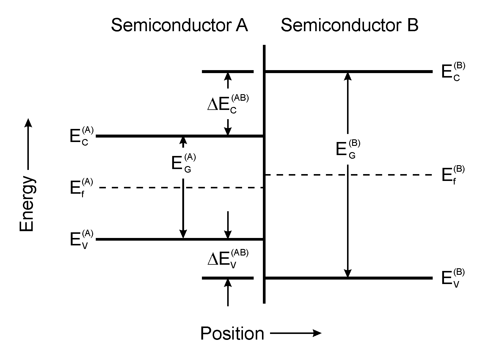
Fig. 3.2 Heterojunction formed between two different semiconductors
By splitting the heterojunction into two separated parts we can easily analyze and understand the formation of the 2DEG. Let’s assume the following that the layer of AlGaN is grown on a GaN buffer. This AlGaN grown layer induces a polarization effect resulting in a positive charge on the AlGaN/GaN interface and a negative charge on the top of the AlGaN layer. This differently charged areas result in forming an electric field inside the AlGaN layer. Next let’s assume that the AlGaN/GaN interface and AlGaN surface are infinitely charged planes, because of very small ratio between the AlGaN layer thickness, which is in order of a few µm and the large side size of the whole substrate.
Firstly let’s analyze the formation of 2Deg in an AlGaN/GaN heterostructure with n-doped AlGaN layer. The polarization described before makes the energy band, including the Fermi level, tilt towards the AlGaN/GaN interface (Fig.3.3 middle). The same effect of energy band tilting can be obtained by making a simple planar capacitor using an n-doped AlGaN as the dielectric and applying voltage on it. Let’s define the negative and positive electrodes of the capacitor. Because of applied voltage an electric force is acting on the free electrons in the layer forcing them to move towards the positive electrode, leaving positive space charges by the negative electrode. After this event the Fermi level is flat again. The built in electric field between the accumulated negative electrons and fixed positive space charges reduces the polarizing electric field making the inclined energy band flatter.
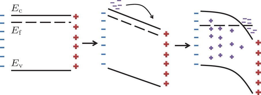
Fig. 3.3 Energy band of freestanding n-doped layer of AlGaN (left), the same layer used as a dielectric for a planar capacitor connected to a voltage source (middle), resulting curved energy band after transportation of free electrons leaving fixed positive charges on the negative electrode of the AlGaN capacitor (right).
Once taking to consideration the connection to GaN layer a fascinating thing will happen. Because the fermi level of GaN is lower of than of AlGaN, accumulated electrons will flow from the lower AlGaN layer to the top of GaN layer forming the resulting 2Deg (Fig.3.4). This process of growing 2Deg will stop when the Fermi levels of both materials will align with each other.
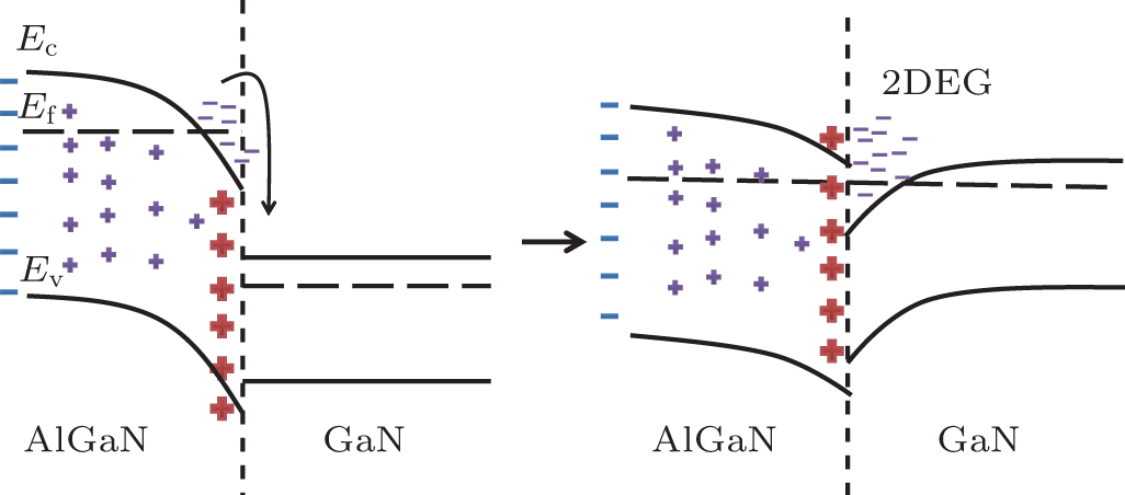
Fig. 3.4 Energy band of an n-doped AlGaN connecting to GaN showing different Fermi layers and electron flow to the GaN material (left), whole energy band of an n-doped AlGaN/GaN heterostructure after equalizing of Fermi levels showing the resulting 2Deg (right).
In real world we don’t need an n-doped AlGaN in order to create 2Deg. With intrinsic AlGaN the situation is different because of few or even no free electrons present in the material. Because of this fact the former method produce many issues, one of little or no electron transport resulting in almost no energy band bending although the tilting remains. Secondly, it can happen that the Fermi level of GaN could be higher than of AlGaN resulting in very few or no electron flow in to the GaN. And because of that no 2Deg should form. But in reality this is not the case.(2)
__________________
| (1) | S. M. Sze , Physics of Semiconductor Devices, John Wiley & Sons, Inc. (1981) |
| (2) | He Xiao-Guang, Zhao De-Gang, Jiang De-Sheng, Formation of two-dimensional electron gas at AlGaN/GaN heterostructure and the derivation of its sheet density expression, Chinese Physics B, 2015, 24(6): 067301 [online] |
Table of contents
Navigation
Site pages
Courses
Archív Elektronika
Settings
Book administration
Course administration