Hi Guest user!
 5 HEMT design and fabrication
5.1 HEMT construction
.
In order to increase RF output power it is necessary to decrease the leakage current resulting from the tunnelling of electrons from the gate metal to the surface of the semiconductor. This can be accomplished by decreasing the magnitude of the electric field at the gate edge.
The use of field plate technology has long been recognized as a useful technique for suppression of voltage at critical locations within a semiconductor device. Schematic figure of GaN/AlGaN HEMT without and with fieldplate is depicted in Fig. 5.1. The field plate consists of an additional metal layer located over the gate metal (Fig. 5.1 right) and extending into the region between the gate and drain. The gate metal provides an electric field termination layer that reduces the magnitude of the field at the gate edge, thereby suppressing the gate leakage current.
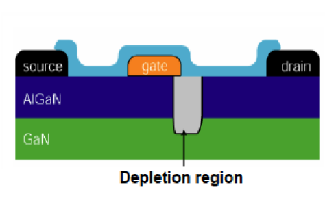
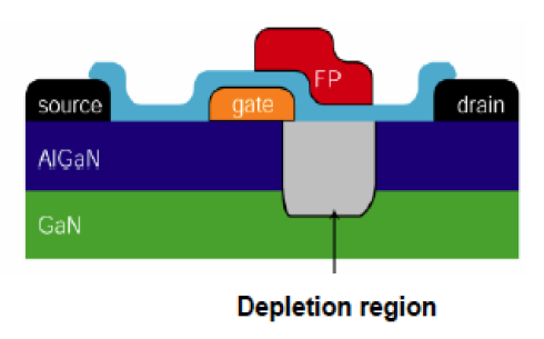
Fig. 5.1 Schematic figure of GaN/AlGaN HEMT without (left) and with (right) fieldplate.
The use of field-plate technology permits high drain bias voltages to be applied, thereby producing improvements in RF output power. In fact, the degree of gate leakage suppression is sufficient to permit drain bias on the order of V DS =100-120 V to be applied. This allows high RF output power to be generated. However, field plates also introduce additional capacitance and reduce the transconductance of the transistor. Therefore a degradation in frequency performance occurs. For this reason, a minimum field-plate length should be employed.(1)
The current in convential HEMT is controlled in a way, that the transistor channel is normally open without gate biased . This makes the implementation of HEMT in electrical circuit very complicated and therefore there are atempts to fabricate a normally off transistor with the same advantages as convential HEMT.
The approach using recessed MIS-gate HEMT designated to be used for power applications is shown on Fig. 5.2 top-left. The epitaxial layers grown on a silicon substrate consist of a buffer layer for relaxing the strain between the substrate and GaN-based layers, an 800-nm-thick AlGaN buffer layer, a 40 nm thick GaN channel layer, 34/1 nm thick AlGaN/AlN barrier layers, and a 1-nm-thick GaN cap layer. The layers of the recessed region were etched by SiCl4/Cl2 using inductively coupled plasma. A maximum field-effect mobility of 120 cm2/Vs and a maximum drain current over 200 mA/mm were attained.(2)
The aproach using fluorine ion implantation of AlGaN barrier designated to be used for RF applications is shown on Fig. 5.2. top-right. Device isolation was carried out by mesa etching with chlorine-based plasma in an inductively coupled plasma reactive ion etching (ICP-RIE) system. After the T-gate windows were opened, the sample was implanted by CF4 plasma in an reactive ion etching (RIE) system with an RF plasma power of 150 W for 150 s. The device exhibits a thresh old voltage of +0.2 V, a saturation drain current density of 735 mA/mm, current-gain cutoff frequency (fT) is closed to 40 GHz, and the power-gain cutoff frequency (fmax) presents more than 90-GHz.(3)
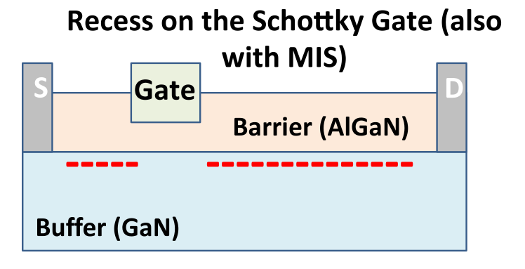
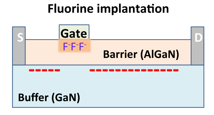
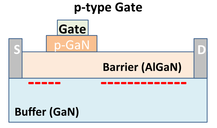
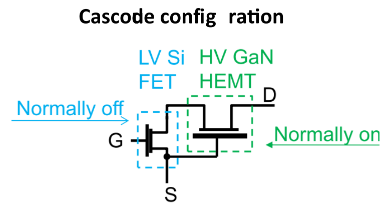
Fig. 5.2 Schematic figures of GaN/AlGaN HEMTs with normally off state using recess on the Schottky gate (top-left), fluorine ion implementation (top-right), p-type gate (bottom-left) and cascode circuit configuration (bottom-right)
The aproach using gate injection transistor (p-gate) designated to be used for switching applications is shown on Fig. 5.2. bottom-right. The gate injection transistor (GIT) utilizes hole injection from the p-type gate to the 2DEG region bringing out the conductivity modulation as observed in insulated-gate bipolar transistors (IGBTs). This new concept enables both normally-off operation and high current driving capability by applying high positive gate voltage with low gate current. A p-AlGaN/i-AlGaN/GaN heteroepitaxial structure for the GIT is grown on a Si substrate with buffer layers consisting of the GaN/AlN multilayers on top of the AlGaN/AlN initial layers. The resulting RON·A and the breakdown voltage are 2.6 mΩ·cm2 and 800 V, respectively. The GIT achieves a high drain current of 200 mA/mm with the threshold voltage of 1.0 V.(4)
In order to achieve a simple normally off state HEMT we can use two separate devices forming a circuit called cascode circuit shown on Fig. 5.2 bottom right. The circuit consist of a low voltage normally of Si field effect transistor (FET) interconnected with normally on GaN HEMT. In this configuration the FET controls the HEMT's gate- source voltage for normally off operation and keeping high voltage capability of HEMT in the same time .
__________________
| (1) | Trew, R.J., Wide bandgap transistor amplifiers for improved performance microwave power and radar applications, 15th International Conference on Microwaves, Radar and Wireless Communications, MIKON - 2004, [online] |
| (2) | T. Oka, T. Nozawa, AlGaN/GaN Recessed MIS-Gate HFET With High-Threshold-Voltage Normally-Off Operation for Power Electronics Applications, IEEE ELECTRON DEVICE LETTERS, VOL. 29, NO. 7, JULY 2008, [online] |
| (3) | Z. H. Feng , R. Zhou, S. Y. Xie, J. Y. Yin, J. X. Fang, B. Liu, W. Zhou, Kevin J. Chen, S. J. Cai, 18-GHz 3.65-W/mm Enhancement-Mode AlGaN/GaN HFET Using Fluorine Plasma Ion Implantation, IEEE Electron Device Letters, Volume:31, Issue: 12, pp. 1386-1388, October 2010, [online] |
| (4) | Y. Uemoto, M. Hikita, H. Ueno, H. Matsuo, H. Ishida, M. Yanagihara, T. Ueda, T. Tanaka, D. Ueda, Gate Injection Transistor (GIT)—A Normally-Off AlGaN/GaN Power Transistor Using Conductivity Modulation, IEEE Transactions on Electron Devices, Volume:54, Issue:12, pp. 3393-3399, Dec. 2007, [online] |
Table of contents
Navigation
Site pages
Courses
Archív Elektronika
Settings
Book administration
Course administration